Ceramic multilayer substrate

a multi-layer substrate and ceramic technology, applied in the direction of printed circuit stress/warp reduction, printed circuit details, non-printed electric components of printed circuits, etc., can solve the problems of cracking at the bottom end of the cavity and deformation, difficult to reduce manufacturing costs, so as to prevent non-uniform deformation

Inactive Publication Date: 2010-06-29
MURATA MFG CO LTD
View PDF20 Cites 1 Cited by
  • Summary
  • Abstract
  • Description
  • Claims
  • Application Information

AI Technical Summary

Benefits of technology

[0011]To overcome the problems described above, preferred embodiments of the present invention provide a ceramic multilayer substrate in which non-uniform deformation is prevented without the addition of a specific process.

Problems solved by technology

In a ceramic multilayer substrate having a cavity, differences in the shrinkage of ceramic layers during firing tend to cause cracks at a bottom end of the cavity and deformation, such as warp or waviness, at a portion forming the bottom of the cavity or a side wall on the perimeter of the cavity.
Hence, it is difficult to reduce the manufacturing costs.
Thus, it is difficult to reduce the manufacturing costs.

Method used


Image

  • Ceramic multilayer substrate
  • Ceramic multilayer substrate
  • Ceramic multilayer substrate

Examples


first preferred embodiment

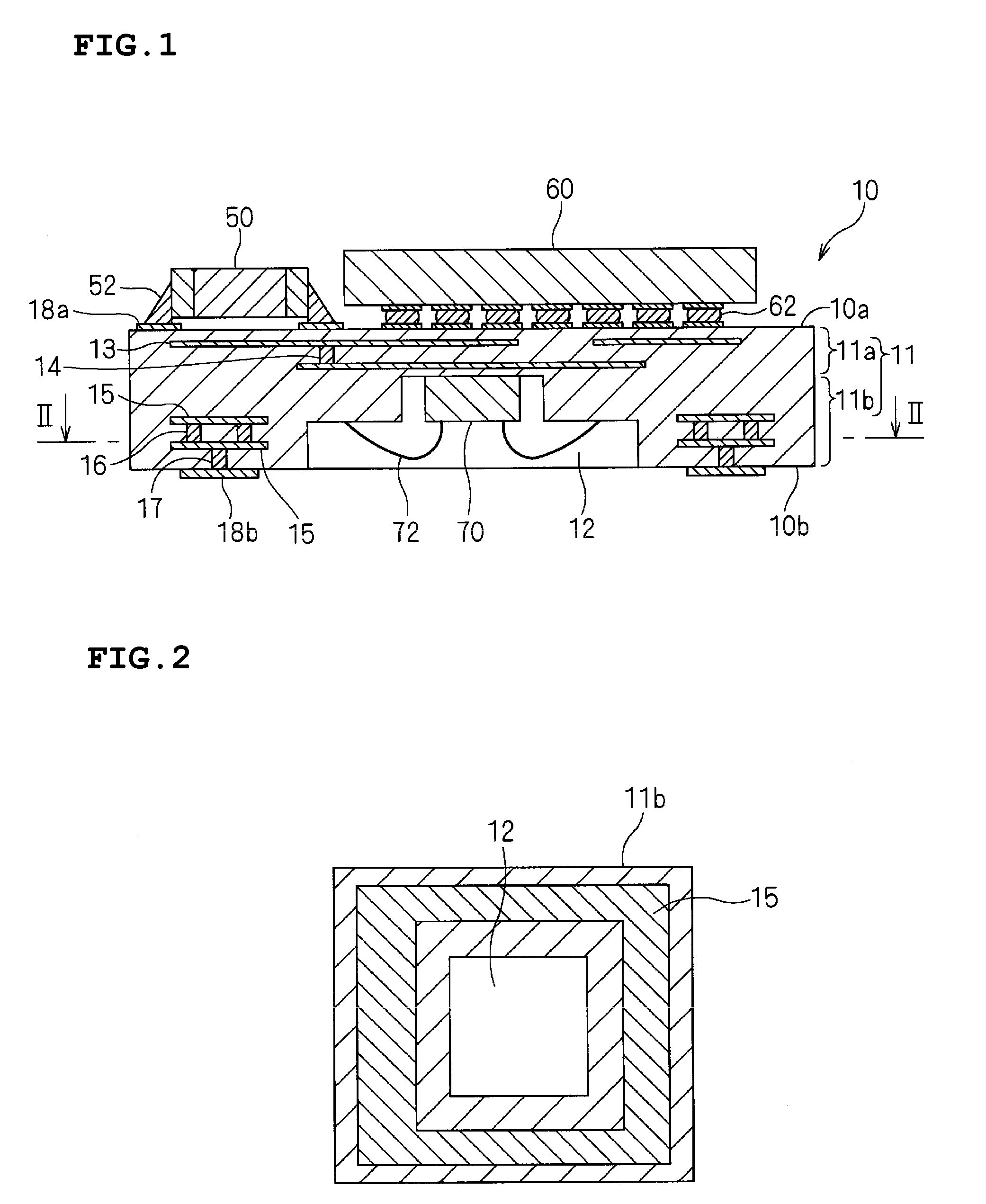
[0056]A ceramic multilayer substrate 10 according to a first preferred embodiment will be described below with reference to FIGS. 1 to 5.

[0057]As illustrated in the cross-sectional view of FIG. 1, a main body 11 of the ceramic multilayer substrate 10 includes a planar base plate portion 11a and a cavity surrounding portion 11b which defines a cavity 12 disposed in the center of the main body 11. The ceramic multilayer substrate 10 is formed by stacking and firing a plurality of ceramic green sheet layers.

[0058]Within the main body 11, an in-plane conductor 13 disposed between ceramic green sheets, a via hole conductor 14 with which a through-hole (via) passing through the ceramic green sheets is filled, and other components define an internal electrode pattern, which defines a portion of a built-in circuit. Examples of the internal electrode pattern include a pattern of a passive element, such as a capacitor or an inductor, a ground pattern, and a wiring pattern for interconnection....

second preferred embodiment

[0082]A ceramic multilayer substrate 20 according to a second preferred embodiment will be described below with reference to FIG. 6.

[0083]The ceramic multilayer substrate 20 has substantially the same inner structure as the ceramic multilayer substrate 10 according to the first preferred embodiment.

[0084]As illustrated in FIG. 6, the ceramic multilayer substrate 20 differs from the ceramic multilayer substrate 10 according to the first preferred embodiment in that, in addition to terminal electrodes 28, surface patterns 26a and 26b are provided on a main surface 20b on a cavity 22 side and that the cavity 22 has a substantially square opening and the main surface 20b of the ceramic multilayer substrate 20 is substantially rectangular and has long sides and short sides.

[0085]When a plurality of terminal electrodes 28 are arranged in a line on the periphery of the main surface 20b, there is space between the opening and short sides 20s (in a direction of long sides 20t) on the main su...

third preferred embodiment

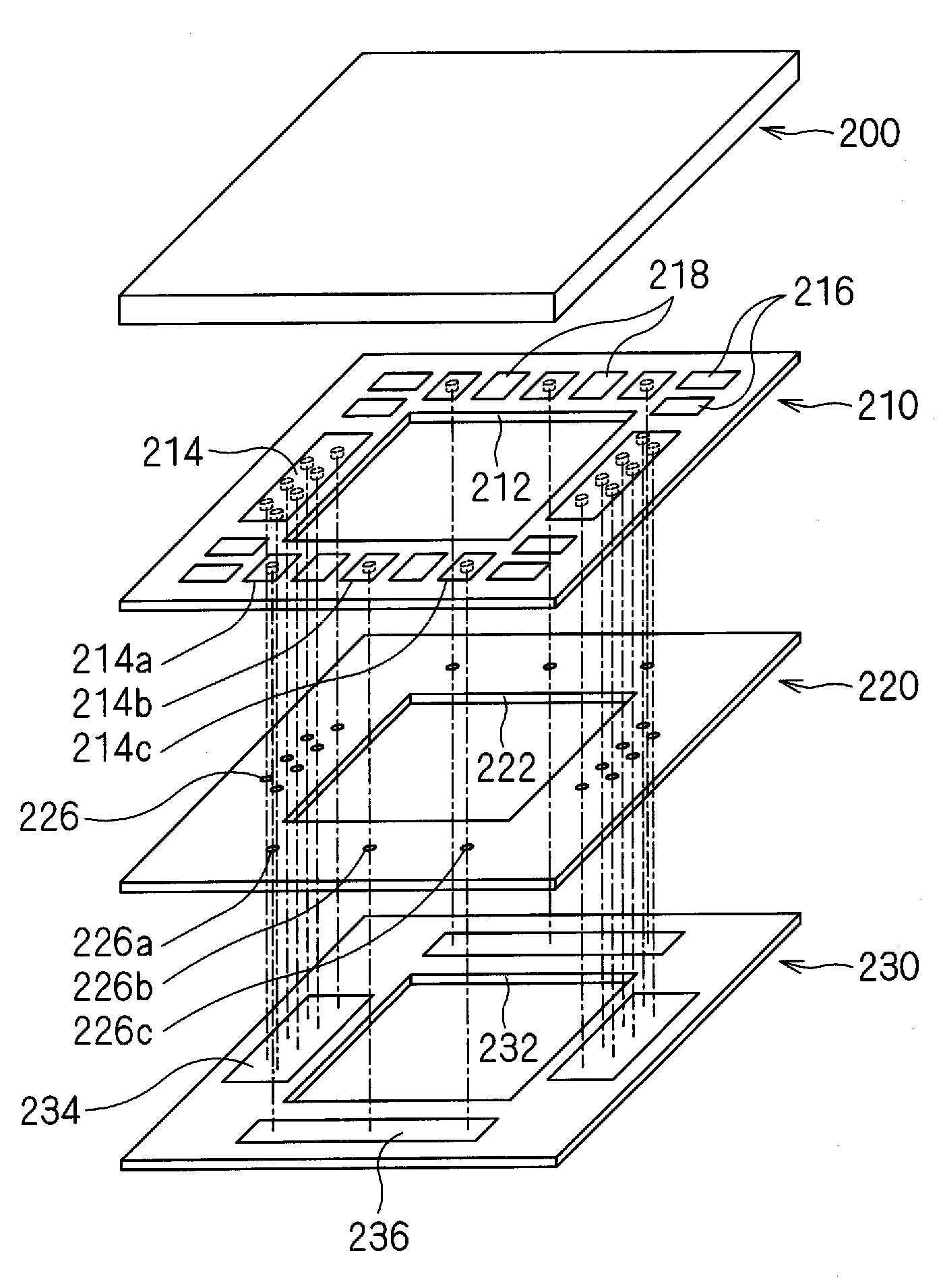
[0088]FIG. 7A is an exploded perspective view of a ceramic multilayer substrate according to a third preferred embodiment. FIG. 7B is an assembly cross-sectional view taken along line b-b of FIG. 7A. In FIG. 7A, a signal line is omitted.

[0089]The ceramic multilayer substrate according to the third preferred embodiment includes laminated ceramic layers 110, 120, and 130 disposed on a planar base plate portion 100. The laminated ceramic layers 110, 120, and 130 have openings 112, 122, and 132, which define a cavity 162.

[0090]The ceramic layers 110 and 130, which are the first layer and the third layer from the base plate portion 100, include deformation preventing patterns 114 and 134. The deformation preventing patterns 114 and 134 are provided on a pair of sides facing each other across the openings 112 and 132 (left and right sides in FIG. 7A). As illustrated in FIG. 7B, the deformation preventing patterns 114 and 134 are connected to each other via interlayer connection conductor ...


PUM

PropertyMeasurementUnit
temperatureaaaaaaaaaa

Abstract

A ceramic multilayer substrate includes a plurality of laminated ceramic layers and at least one conductor pattern and disposed on at least one of the ceramic layers. The ceramic multilayer substrate has a cavity in at least a first main surface. The ceramic multilayer substrate includes a deformation preventing pattern disposed on at least one of the ceramic layers having an opening forming the cavity. The deformation preventing pattern surrounds the entire perimeter of the opening and is made of the same material as the conductor pattern.

Description

BACKGROUND OF THE INVENTION[0001]1. Field of the Invention[0002]The present invention relates to a ceramic multilayer substrate, and more particularly, to a ceramic multilayer substrate having a cavity.[0003]2. Description of the Related Art[0004]A ceramic multilayer substrate having a cavity structure has been used to increase the packaging density and to reduce the size and the profile of an electronic component.[0005]A ceramic multilayer substrate having a cavity is formed by stacking a green ceramic layer having no opening and a green ceramic layer having an opening and firing them to form a cavity. In a ceramic multilayer substrate having a cavity, differences in the shrinkage of ceramic layers during firing tend to cause cracks at a bottom end of the cavity and deformation, such as warp or waviness, at a portion forming the bottom of the cavity or a side wall on the perimeter of the cavity. Various techniques have been proposed to prevent such failures.[0006]For example, Japan...

Claims


Application Information

Patent Timeline
Patent Type & Authority Patents(United States)
IPC IPC(8): H05K1/03
CPCH01L23/15H01L23/49827H05K1/0271H05K1/183H01L23/49822H01L2924/19106H01L2224/48091H01L2924/01004H01L2924/01046H01L2924/01079H01L2924/09701H01L2924/15153H01L2924/1517H01L2924/1532H01L2924/19041H01L2924/19105H01L2924/3025H05K1/0298H05K1/0306H05K2201/09481H05K2201/09781H01L2224/16225H01L24/48H01L2924/00014H01L2924/12042H01L2924/14H01L2224/05573H01L2224/05568H01L2924/00H01L2224/05599H01L2224/45099H01L2224/45015H01L2924/207H05K3/46
Inventor ISEBO, KAZUHIRO
Owner MURATA MFG CO LTD
Why Eureka
Try Eureka