Light emitting device with silicone resin layer formed by screen printing

a technology of silicone resin and light-emitting device, which is applied in the direction of thermoelectric devices, discharge tubes/lamp details, discharge tubes luminescnet screens, etc., can solve the problems of resin bleedout of low molecular weight, affecting the mechanical strength prone to deterioration of the main skeleton of the cured product, etc., to achieve excellent heat resistance and light resistance, excellent optical transparency, and superior mechanical strength

Active Publication Date: 2010-06-29
NICHIA CORP
View PDF13 Cites 228 Cited by
  • Summary
  • Abstract
  • Description
  • Claims
  • Application Information

AI Technical Summary

Benefits of technology

[0007]Accordingly, an object of the present invention is to provide a light emitting device, in which the light emitting element exhibits excellent levels of heat resistance, light resistance to high energy light such as ultraviolet light, and mechanical strength, and has been coated with a silicone resin layer that is suited to formation using a screen printing method.
[0015]The silicone resin composition used in coating the light emitting element of a light emitting device of the present invention contains no silethylene linkages within the cured product, and consequently exhibits excellent levels of heat resistance and light resistance, as well as superior mechanical strength, excellent optical transparency, and a small birefringence.
[0016]Furthermore, because the resin layer is formed by screen printing, the uniformity of the film thickness is excellent, meaning color irregularities during light emission from the light emitting element are unlikely. Additional benefits include the fact that the resin composition used is easily separated from the mask such as a metal mask used during screen printing, and the fact that following curing, the composition exhibits excellent adhesion to the light emitting element, and a high level of durability.
[0017]Accordingly, a light emitting device of the present invention is able to exhibit stable optical characteristics and a high level of reliability over an extended period.

Problems solved by technology

Because silethylene linkages are prone to cleavage by light or heat, the main skeleton within the cured product is prone to deterioration, and the resin is prone to bleed-out of low molecular weight, fluid, oily silicone.
As a result, the mechanical strength of the cured product falls, and the resin is more likely to become brittle and prone to heat deformation.
Furthermore, the low molecular weight silicone components that bleed out can cause a variety of faults.
In addition, if the resin reaches this state, then color irregularities and tone variation are more likely to occur during light emission, meaning the color tone characteristics of the light emitting element may be affected.
However, the uniformity of the film thickness of a resin layer formed using this method is poor, which can cause color irregularities during light emission.
In a screen printing method, the resin used should exhibit ready separation from the metal mask during printing, and superior adhesion to the light emitting element following curing, but a resin material that adequately satisfies these requirements is, as yet, still unknown.

Method used


Image

  • Light emitting device with silicone resin layer formed by screen printing
  • Light emitting device with silicone resin layer formed by screen printing
  • Light emitting device with silicone resin layer formed by screen printing

Examples


embodiments

[0099]Next is a description of a specific embodiment of a light emitting device of the present invention.

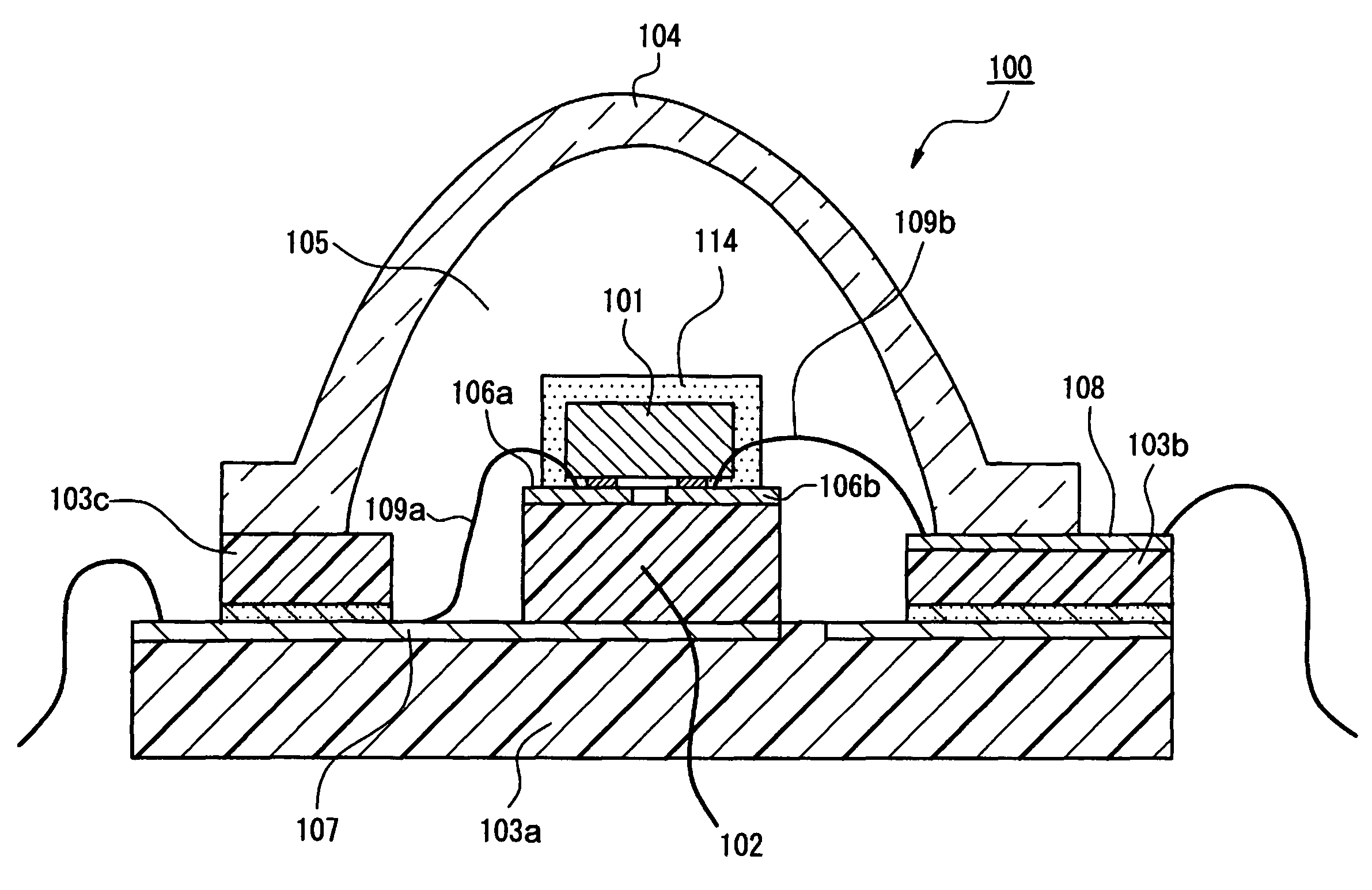
[0100]FIG. 1 is a schematic cross-sectional view through a cross section perpendicular to the principal surface (the surface on which the element is mounted) of a support of a light emitting device 100 according to the present embodiment. In order to facilitate the description, the dimensions of each of the structural components and members have been magnified, so that the figure does not necessarily represent actual dimensions or relative sizes.

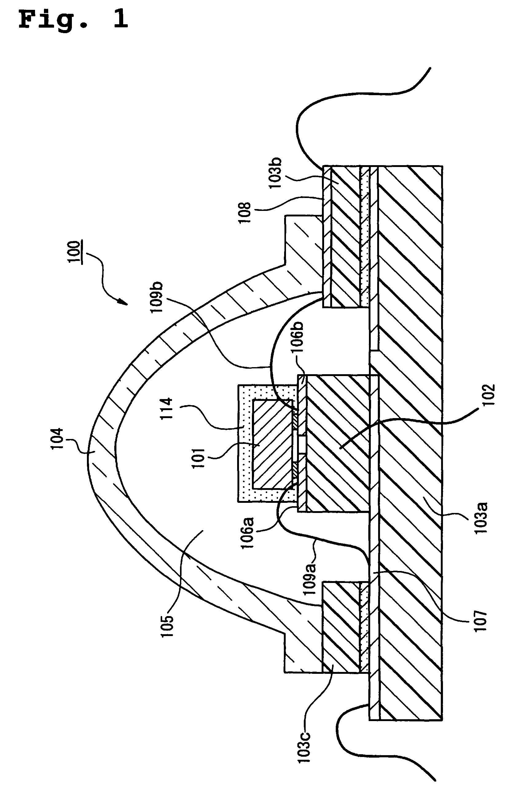
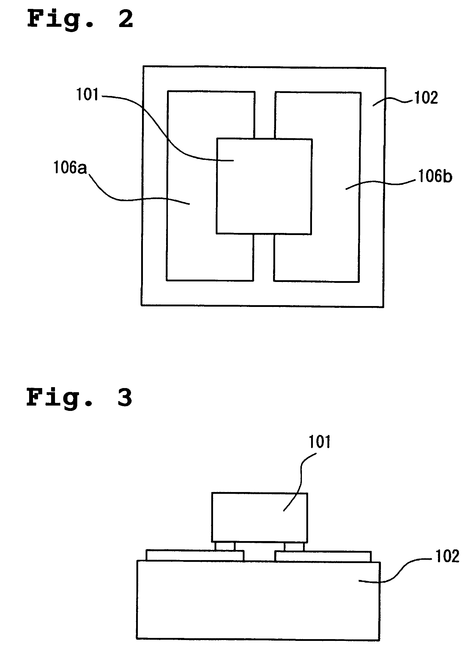
[0101]The light emitting device 100 has a sub-mount 102 to which a light emitting element 101 is flip-chip mounted, a support 103a for supporting the sub-mount 102, and a glass lens 104 which is a transparent member positioned on the principal surface side of the support 103a. The glass lens 104 is a hemispherical shaped lens, which has a convex shape when viewed from above the light emitting device 100 in the direction of the light emitt...

synthesis examples

[0109]The methyltrimethoxysilane used in Synthesis Examples described below is KBM13 (a brand name) manufactured by Shin-Etsu Chemical Co., Ltd., and the dimethyldimethoxysilane is KBM22 (a brand name), also manufactured by Shin-Etsu Chemical Co., Ltd.

synthesis example 1

[0110]A stirrer and a condenser tube were fitted to a 1 L three-neck flask. This flask was then charged with 109 g (0.8 mols) of methyltrimethoxysilane, 24 g (0.2 mols) of dimethyldimethoxysilane, and 106 g of isobutyl alcohol, and the mixture was cooled in ice with constant stirring. With the temperature inside the reaction system maintained at 0 to 20° C., 60.5 g of a 0.05 N hydrochloric acid solution was added dropwise. Following completion of the dropwise addition, the reaction mixture was stirred for 7 hours under reflux at 80° C. Subsequently, the reaction solution was cooled to room temperature, and 150 g of xylene was added to dilute the reaction solution. The reaction solution was then poured into a separating funnel, and washed repeatedly with 300 g samples of water until the electrical conductivity of the separated wash water fell to no more than 2.0 μS / cm. The water was then removed from the washed reaction solution by azeotropic distillation, and following adjustment of...


PUM

PropertyMeasurementUnit
thicknessaaaaaaaaaa
temperatureaaaaaaaaaa

Abstract

A light emitting device, including a light emitting element, and a resin layer that has been screen printed to coat said light emitting element is provided. The resin layer is formed from a curable silicone resin composition, which includes (i) an organopolysiloxane with a polystyrene equivalent weight average molecular weight of at least 5×10³, (ii) a condensation catalyst, (iii) a solvent, and (iv) a finely powdered inorganic filler. The uniformity of the film thickness is excellent, thus resulting in little color irregularities during light emission from the light emitting element.

Description

BACKGROUND OF THE INVENTION[0001]1. Field of the Invention[0002]The present invention relates to a light emitting device that can be used in a liquid crystal backlight, an illumination light source, and various types of indicators, displays and traffic signal lights, and relates particularly to a light emitting device in which the light emitting element is coated with a silicone resin.[0003]2. Description of the Prior Art[0004]In light emitting devices that use a light emitting element such as an LED, the light emitting element is typically coated with a phosphor-containing layer, or a transparent resin layer that functions as a lens or the like. Conventionally, epoxy resins have been used as the material for these coating layers, but recently, silicone resins have begun to attract attention, as a result of their superior levels of heat resistance.[0005]However, with short wavelength LEDs such as blue LEDs and ultraviolet LEDs now being developed, the resin layer now requires a toug...

Claims


Application Information

Patent Timeline
Patent Type & Authority Patents(United States)
IPC IPC(8): H01L35/24H01L51/00H01L33/56
CPCC09D183/04H01L33/56C09D183/06H01L2224/16H01L2924/00014H01L2924/00011H01L2224/0401
Inventor SOFUE, SHINSUKETAMAKI, HIROTOIZUNO, KUNIHIRO
Owner NICHIA CORP
Why Eureka
Try Eureka