
Correcting offset in magneto-resistive devices

a technology of offset correction and magnetic resistance, applied in the field of anisotropic magnetoresistive sensors, can solve the problems of inability to accurately detect the current value, the circuit to be physically larger and operationally slower, and the sensor type has an inherent offset bias voltage, etc., to facilitate the use of amr sensors, reduce manufacturing costs, and operate less power

Active Publication Date: 2010-07-13
ACEINNA TRANSDUCER SYST CO LTD
View PDF12 Cites 8 Cited by
  • Summary
  • Abstract
  • Description
  • Claims
  • Application Information

AI Technical Summary

Benefits of technology

[0012]The present invention thus facilitates use of an AMR sensor without having to do significant additional processing to calculate the field strength of an applied magnetic field. This permits use of the AMR sensor as a direct replacement for the more common fluxgate (or flux-valve) magnetometer that produces a voltage proportional to an applied external field, and without having to perform set and reset calculations. This elimination of offset bias is independent of temperature and demonstrates the importance of the present invention, for example, for magnetic compassing where accurate angles are necessary. In addition, the present invention costs significantly less than conventional fluxgate designs and requires much less power to operate. Offset bias is thus removed in accordance with the present invention, with concurrent reductions in manufacturing costs compared with most fluxgate designs that require either special design considerations or temperature calibration to remove offset bias.

Problems solved by technology

However, this type of sensor has an inherent offset bias voltage caused by mismatches within the resistive bridge.
This offset current is selected for each individual device and selecting the current value can be time consuming for devices used in systems that are mass produced.
This scheme requires extra components and causes the circuit to be physically larger and operationally slower.
Another scheme to reduce the offset includes a servo mechanism which adds complexity and reduces bandwidth due to roll-off response of the integrator involved.
A general rule of thumb for clock to integrator cutoff frequencies is 10 times. This limits the useful bandwidth of the sensor.
The downside of increasing the clock frequency is the power consumption increases and self heating of the sensor bridge may start to affect the operation of the circuit.
Some schemes can also reduce the available bandwidth or resolution of the sensor circuit.
In the digital subtraction scheme, there is also a loss in dynamic range caused by the subtraction of the Vset and Vreset voltages.
Several known schemes of bias reduction all have various draw backs either reducing the dynamic range, using extra measurements to calculate the bias, or various other problems.

Method used


Image

  • Correcting offset in magneto-resistive devices
  • Correcting offset in magneto-resistive devices
  • Correcting offset in magneto-resistive devices

Examples


Embodiment Construction

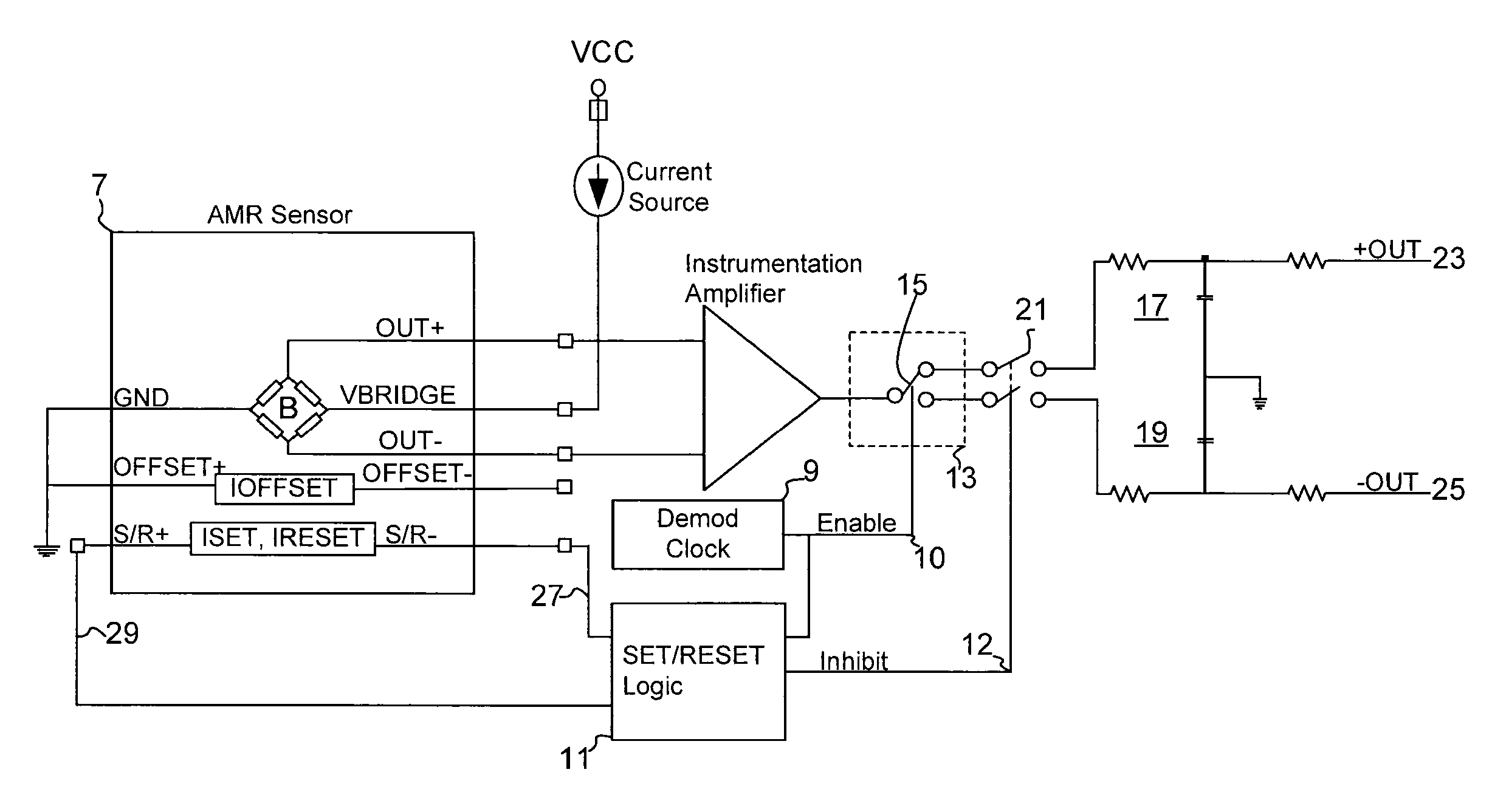
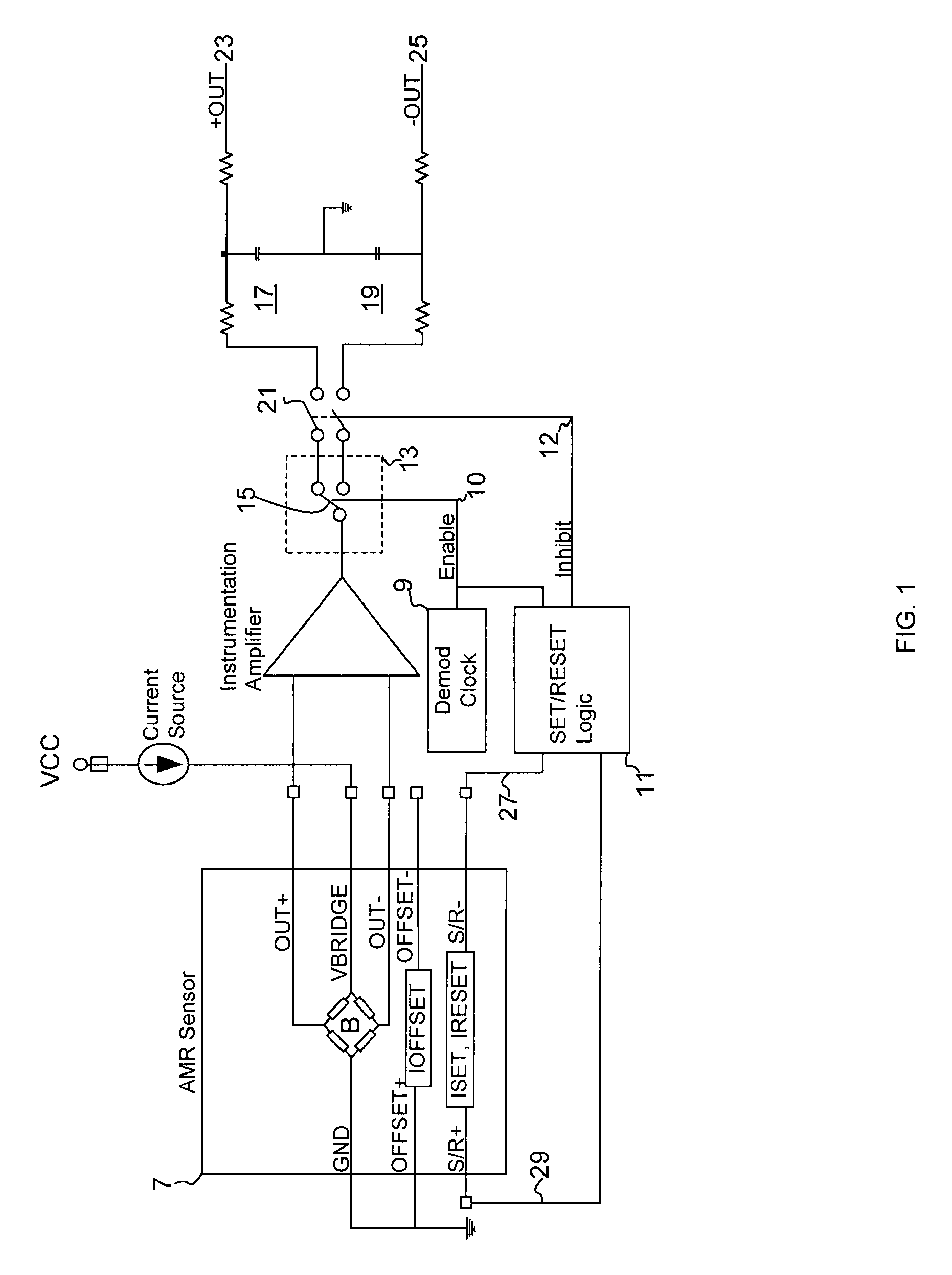
[0015]Referring now to the block diagram in FIG. 1, there is shown a block schematic diagram of one embodiment of the present invention including a commutating demodulator. The demodulator clock drives the set and reset circuits 11 as well as a flip-flop circuit 13 that controls the commutating switch 15. The output of the switch 15 supplies two integrators 17, 19 that derive the differential signal. An inhibit switch 21 turns off the output signal from circuit 13 when the SET / RESET signal is present to eliminate this signal passing through to the outputs 23, 25.

[0016]This embodiment of the present invention allows direct measurements to be made from the sensor 7 in contrast to conventional schemes that require several intermediate measurements to be made to calculate sensor offset in order to correct the sensor output. In this embodiment, the sensor offset is removed by the commutating demodulator circuit of FIG. 1 that produces the sensor output as the differential signal 23, 25 a...


PUM


Abstract

Method and apparatus improve sensing accuracy and reduce bias shift in anisotropic magneto-resistive sensors using paired integrators and sampling switches for processing outputs of the sensor on applied set and reset signals with high immunity to temperature variations.

Description

FIELD OF THE INVENTION[0001]This invention relates to anisotropic magneto-resistive sensors, and more particularly to apparatus and method for reducing bias offset and temperature sensitivity in such sensors operating in host systems.BACKGROUND OF THE INVENTION[0002]Anisotropic magneto-resistive (AMR) sensors are used in many devices from compasses to steering and positioning devices. These sensors include resistive bridges to provide accurate measurements of weak magnetic fields. (See, for example, U.S. Pat. No. 5,519,318). However, this type of sensor has an inherent offset bias voltage caused by mismatches within the resistive bridge. One scheme for removing this offset is to provide an offset current back into an amplifier connected to the bridge. This offset current is selected for each individual device and selecting the current value can be time consuming for devices used in systems that are mass produced.[0003]Another scheme to reduce the offset is to correct it in the digit...

Claims


Application Information

Patent Timeline
Patent Type & Authority Patents(United States)
IPC IPC(8): G01B7/14G01R33/02
CPCG01R33/0029G01R33/02
Inventor JAMES, JOHN J
Owner ACEINNA TRANSDUCER SYST CO LTD
Learn More