
Semiconductor structure and method of manufacturing a semiconductor structure

a semiconductor and semiconductor technology, applied in the field of semiconductor structure, can solve problems such as strain-induced dislocations in the structure formation, and achieve the effects of low diffusion region thickness, effective light diffusion capability, and convenient processing

Inactive Publication Date: 2010-07-27
OPTOGAN OY
View PDF12 Cites 1 Cited by
  • Summary
  • Abstract
  • Description
  • Claims
  • Application Information

AI Technical Summary

Benefits of technology

"The present invention is a semiconductor structure that includes a bottom cladding layer, a diffusion region, and a top cladding layer. The diffusion region has a refractive index different from that of the cladding layers and non-flat surfaces to form light diffusing interfaces. The non-flat surfaces help improve the brightness of the light emitting device layers grown on top of the structure. The refractive index difference between the diffusion region and the cladding layers enhances the diffusion efficiency. The structure is formed without introducing strain-induced dislocations and has enhanced light diffusing capability. The invention also provides a method for manufacturing the semiconductor structure. The technical effects of the invention include improved brightness of light emitting devices and reduced dislocation-related degradation of device layers."

Problems solved by technology

Different lattice constants of the cladding layers could cause formation of strain-induced dislocations in the structure.

Method used


Image

  • Semiconductor structure and method of manufacturing a semiconductor structure
  • Semiconductor structure and method of manufacturing a semiconductor structure
  • Semiconductor structure and method of manufacturing a semiconductor structure

Examples


Embodiment Construction

[0027]Reference will now be made in detail to the embodiments and examples relating to the present invention, which are illustrated in the accompanying figures.

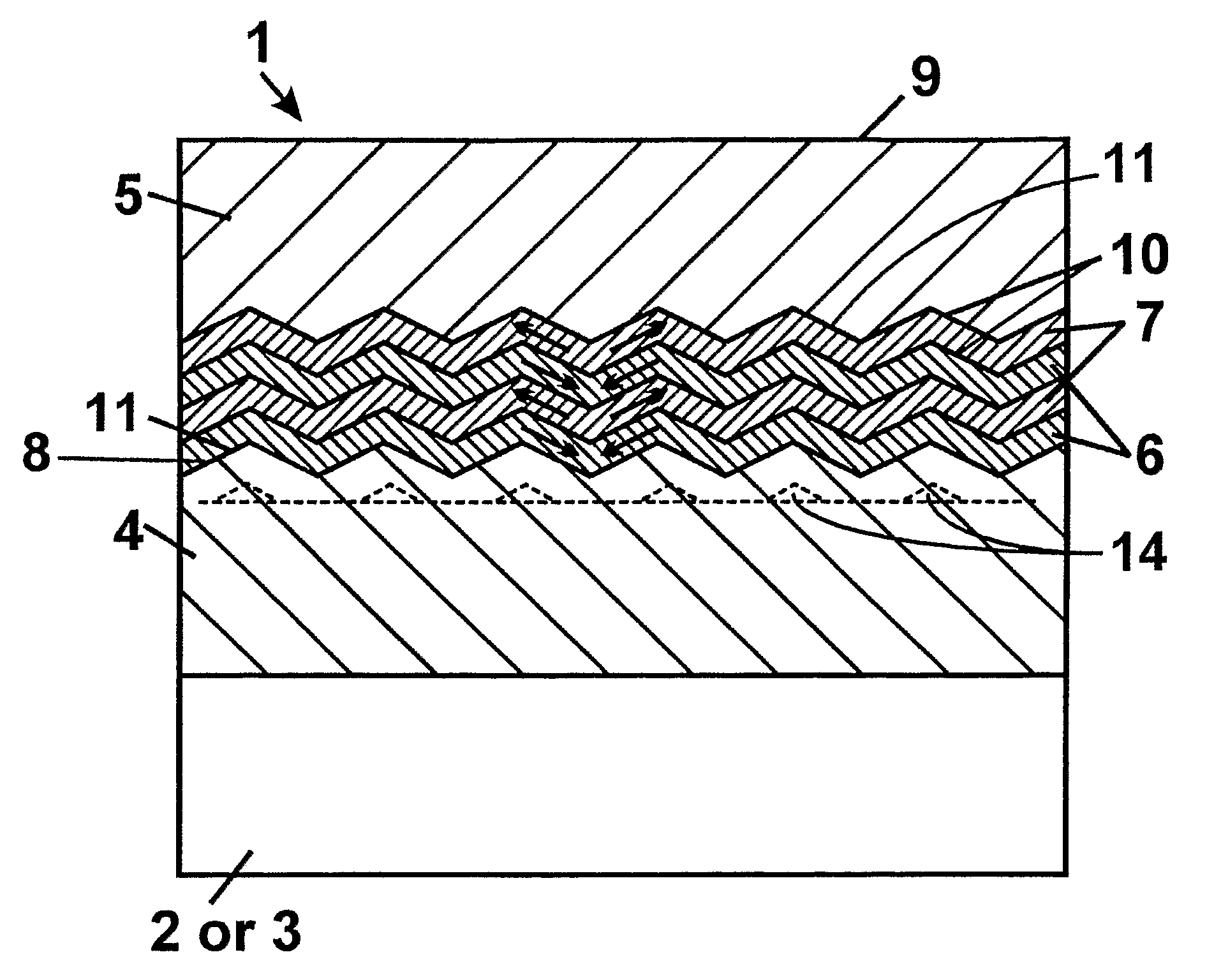
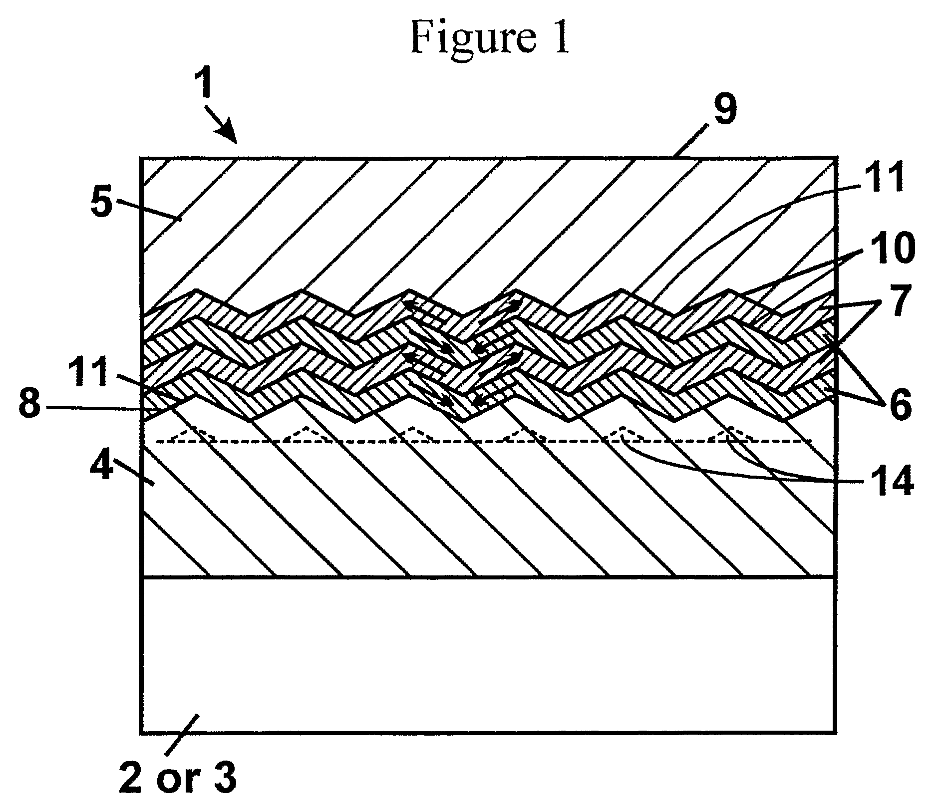
[0028]The semiconductor structure 1 of FIG. 1 comprises a substrate 2 formed of the semiconductor structure materials or substrate 3 formed of foreign materials, a bottom cladding layer 4 with a surface 8 having facets 11 with crystallographic indexes other than (0001) and those of the type {1 100}, a top cladding layer 5 with flat surface 9, and a diffusion region consisting of two pairs of first diffusion layer 6 and second diffusion layer 7. Dashed line shows the precipitates 14 grown during the growing of the bottom cladding layer. The top cladding layer has a lattice constant equal to that of the bottom cladding layer. The diffusion layers have refractive indices different from those of the cladding layers. In addition, the refractive index of the first diffusion layers 6 is different from that of the second diffusion la...


PUM


Abstract

A semiconductor structure is formed of nitrides of group III metals having wurtzite crystal structure and grown in vapor phase on a (0001) oriented semiconductor substrate. The structure comprises a bottom cladding layer, a top cladding layer, and a diffusion region positioned between the cladding layers for diffusing light propagating within the semiconductor structure. The diffuse region has refractive index different from those of the cladding layers and non-flat surfaces for providing light diffusing interfaces between the diffusion region and the cladding layers. According to the invention, the diffusion region comprises a plurality of diffusion layers, compositions and thicknesses of said diffusion layers having been chosen to avoid formation of strain-induced dislocations in the diffusion region, and adjacent diffusion layers having different refractive indices in order to further enhance the diffusion efficiency.

Description

FIELD OF THE INVENTION[0001]The invention relates in general to a semiconductor structure with enhanced light diffusion capability to be used as a part of a light emitting device. More particularly, the semiconductor structure is formed of nitrides of group III metals with wurtzite crystal structure and grown in vapor phase on a (0001) oriented substrate, formed either of the semiconductor structure materials or of foreign materials. The invention also relates to a method of manufacturing such structure.BACKGROUND OF THE INVENTION[0002]Design of a semiconductor structure for light emitting diodes influences on overall efficiency of the diodes through two main parameters: efficiency of conversion of electrical power to optical power in light generation region and efficiency of emission of light generated in this region from the structure. In a light emitting structure made of nitrides of group III metals grown in vapor phase on foreign substrate with refractive index less than that o...

Claims


Application Information

Patent Timeline
Patent Type & Authority Patents(United States)
IPC IPC(8): H01L21/02H01L33/00H01L33/24
CPCH01L33/24H01L33/007H01L33/32H01L33/20
Inventor BOUGROV, VLADISLAV E.ODNOBLYUDOV, MAXIM A.
Owner OPTOGAN OY
Learn More