
Method for semiconductor compositional grading to realize low-resistance, distributed Bragg reflectors

a technology of distributed bragg reflectors and compositional grading, which is applied in the direction of semiconductor lasers, polycrystalline material growth, crystal growth process, etc., can solve the problems of reducing the optical performance of the mirror, presenting challenges, and affecting the stability of the semiconductor composition, so as to improve the optical and electrical characteristics

Active Publication Date: 2010-08-03
OC ACQUISITION CORP
View PDF4 Cites 25 Cited by
  • Summary
  • Abstract
  • Description
  • Claims
  • Application Information

AI Technical Summary

Benefits of technology

[0014]In accordance with a first aspect of the invention, a method of manufacturing a distributed Bragg reflector (DBR) in AIIIBV compounds with improved optical and electrical characteristics is provided. The method involves a growth apparatus containing multiple group III elements and a group V element, and including multiple sources of at least one of said multiple group-III elements (AIII) in the AIIIBV compound, and which have select...

Problems solved by technology

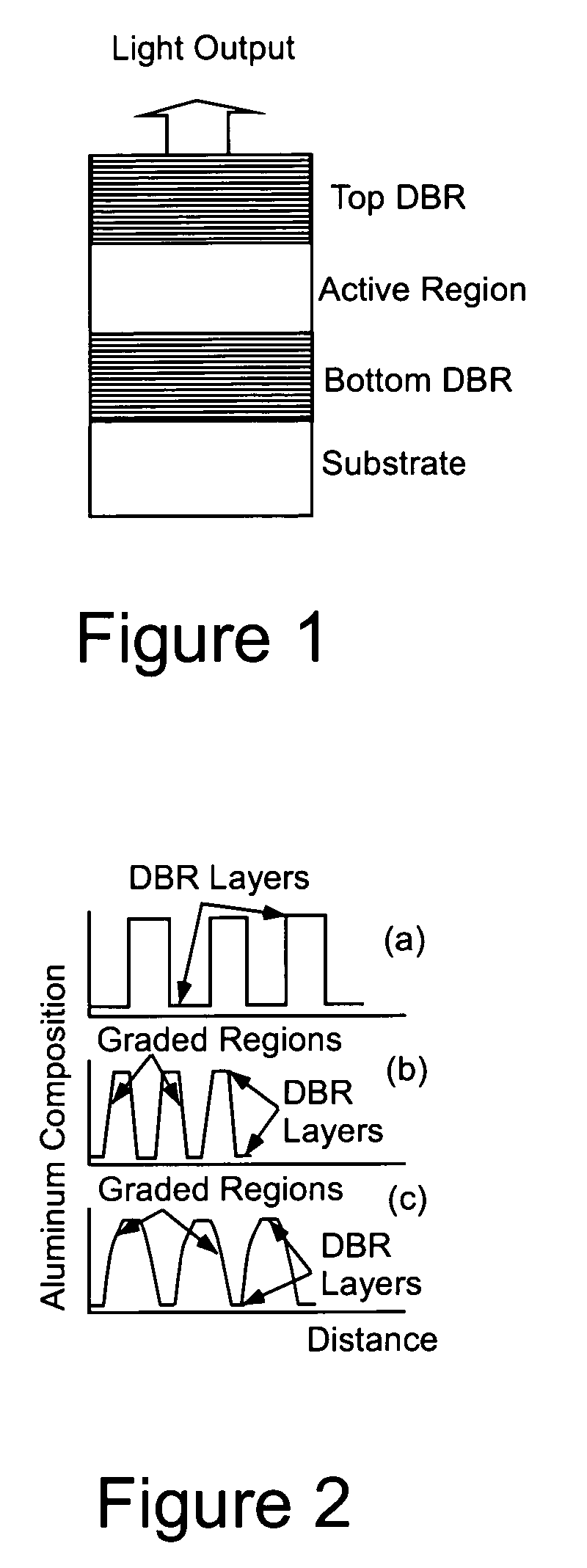
However, good electrical performance, e.g., having low electrical resistance, often requires changes in the DBR structure that will reduce the optical performance of the mirror.
This different growth methodology presents challenges when trying to realize analog grading schemes, as described above, using MOCVD.
Thus, accurate, dynamic control of the flux can be problematic.
This will likely accelerate the failure of the shutters, and involve costly system maintenance.
However, the thickness of the layers within the superlattice is small enough to allow significant tunneling of carriers through these energy barriers, resulting in low-resistance DBRs using this method.

Method used


Image

  • Method for semiconductor compositional grading to realize low-resistance, distributed Bragg reflectors
  • Method for semiconductor compositional grading to realize low-resistance, distributed Bragg reflectors
  • Method for semiconductor compositional grading to realize low-resistance, distributed Bragg reflectors

Examples


Embodiment Construction

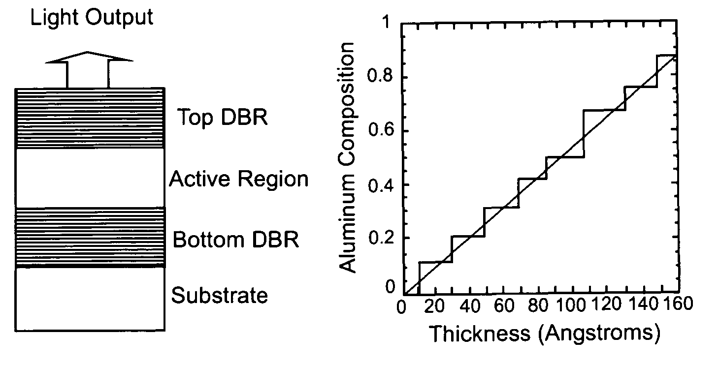
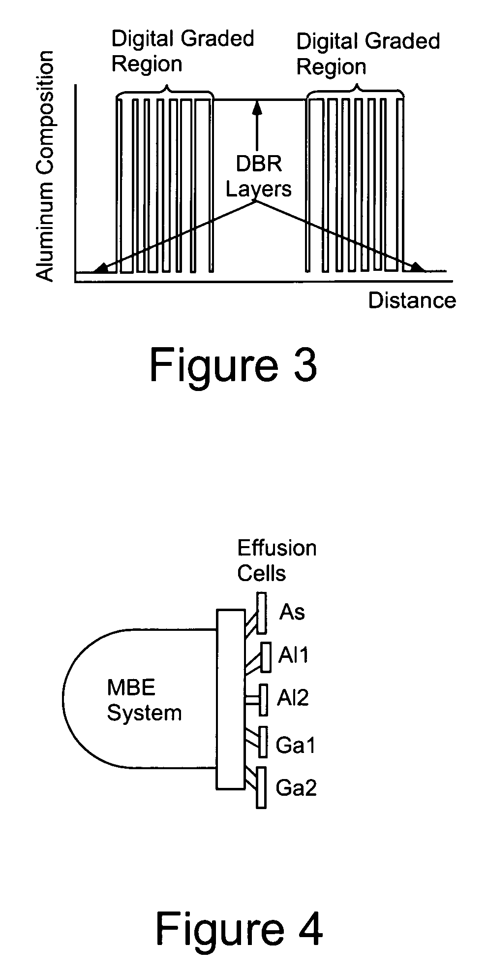
[0042]The proposed method for compositional grading employs a concept, involving the combination of thin, discrete, layers, to realize a compositional grade. However, this method differs from the digital alloy scheme described above in that this process employs small layers, each with a different AlxGa1-xAs composition, to approximate an analog compositional grading scheme. This method uses MBE and requires a system with multiple group-III elemental sources, as shown in FIG. 4. For the purposes of this explanation, the MBE system is configured with three Al sources and two Ga sources. However, other multi-source configurations can be used to realize this novel process. This method can be used in multiple material systems, but for the purposes of this description, the AlxGa1-xAs material system will be used. Using various combinations of the elemental Ga- and Al-sources, each with a different flux rate, different AlxGa1-xAs compositions can be realized for use in the graded DBR struc...


PUM


Abstract

A method of manufacturing a distributed Bragg reflector (DBR) in group III-V semiconductor compounds with improved optical and electrical characteristics is provided. A selected DBR structure is achieved by sequential exposure of a substrate to predetermined combinations of the elemental sources to produce a pair of DBR layers of compound alloys and a graded region including one or more discrete additional layers between the DBR layers of intermediate alloy composition. Exposure durations and combinations of the elemental sources in each exposure are predetermined by DBR design characteristics.

Description

PRIORITY[0001]This application claims the benefit of priority to U.S. provisional patent application Ser. No. 60 / 548,502, filed Feb. 26, 2004.GOVERNMENT INTERESTS[0002]The United States Government has a paid-up license in this invention and the right in limited circumstances to require the patent owner to license others on reasonable terms as provided by the terms of Contract No. F29601-03-C-0030 awarded by the United States Air Force Research Laboratory.BACKGROUND[0003]1. Field of the Invention[0004]The invention relates to distributed Bragg reflectors (DBRs), and particularly to a DBR manufactured with a compositional grading scheme and exhibiting low resistance.[0005]2. Description of the Related Art[0006]The need for increasing data-transfer capacity has led to the development of high-performance optoelectronic components, including vertical-cavity, surface-emitting lasers (VCSELs). VCSELs consist of an active region located between two highly-reflective mirrors, as shown in FIG...

Claims


Application Information

Patent Timeline
IPC IPC(8): H01L21/00
CPCC30B23/02C30B29/40C30B29/42H01S5/18344H01S2304/02
Inventor PICKRELL, GREGORYLOUDERBACK, DUANE A.GUILFOYLE, PETER
Owner OC ACQUISITION CORP
Learn More