Bus system

a bus system and bus technology, applied in the field of distributed bus systems, can solve the problems of insufficient embedded systems, tri-state buses or wired-or buses, which are used, and increase signal delays, so as to reduce the number of interconnections, shorten the delay time, and reduce the load

Inactive Publication Date: 2010-08-17
SAMSUNG ELECTRONICS CO LTD
View PDF5 Cites 0 Cited by
  • Summary
  • Abstract
  • Description
  • Claims
  • Application Information

AI Technical Summary

Benefits of technology

[0009]It is another object of the present invention to provide a bus system operable with less number of interconnections.
[0010]It is a further object of the present invention to provide a bus system operable with less length of interconnection lines.
[0016]In accordance with the invention, a reduction of the number of interconnections is achieved. In other word, interconnection numbers are reduced to M from M*N. As can be appreciated, number M is smaller than the number of the centralized single MUXs and smaller than the tri-state buses. Such a decrease in the number of interconnections is desirous for shortening signal delay times that are due to mutual interferences. Furthermore, the decrease is desirous for a reduction of the area of a chip. Second, the instant invention increases signal propagation speed and lowers power consumption rate. Since buses of the instant invention transfer signals in one direction, it is sufficient just to consider only the loads along the direction, while the conventional tri-state buses conduct bi-directional signal transmission, which necessarily means that consideration of the entire loads over all of the buses is required. Therefore, the smaller load in transferring signals causes the lower power consumption. Third, operational timing is optimally controlled in a bus system of the invention. Since there are differences in delay times between the data sources in accordance with their connecting positions to buses, coupled with the condition of the unidirectional signal transmission, data sources with smaller delay times can be placed at positions closer to data sinks corresponding thereto. Forth, the present invention does not need additional buffers because the OR gate associated with the bus also performs the function carried out by the conventional buffers. This feature reduces delays through interconnections on buses.

Problems solved by technology

However, many problems occur when the MUX-based buses are coupled to conventional MUX cells.
Since a practical system employs numerous MUXs, the mutual interferences between the multiplicity of interconnections can cause increased signal delays.
Based upon usage and prior experiments, tri-state buses or wired-OR buses, which are used in large quantity in high-end processors, are regarded as insufficient for embedded systems such a SOC because of difficulties in testing.

Method used


Image

  • Bus system
  • Bus system
  • Bus system

Examples


first embodiment

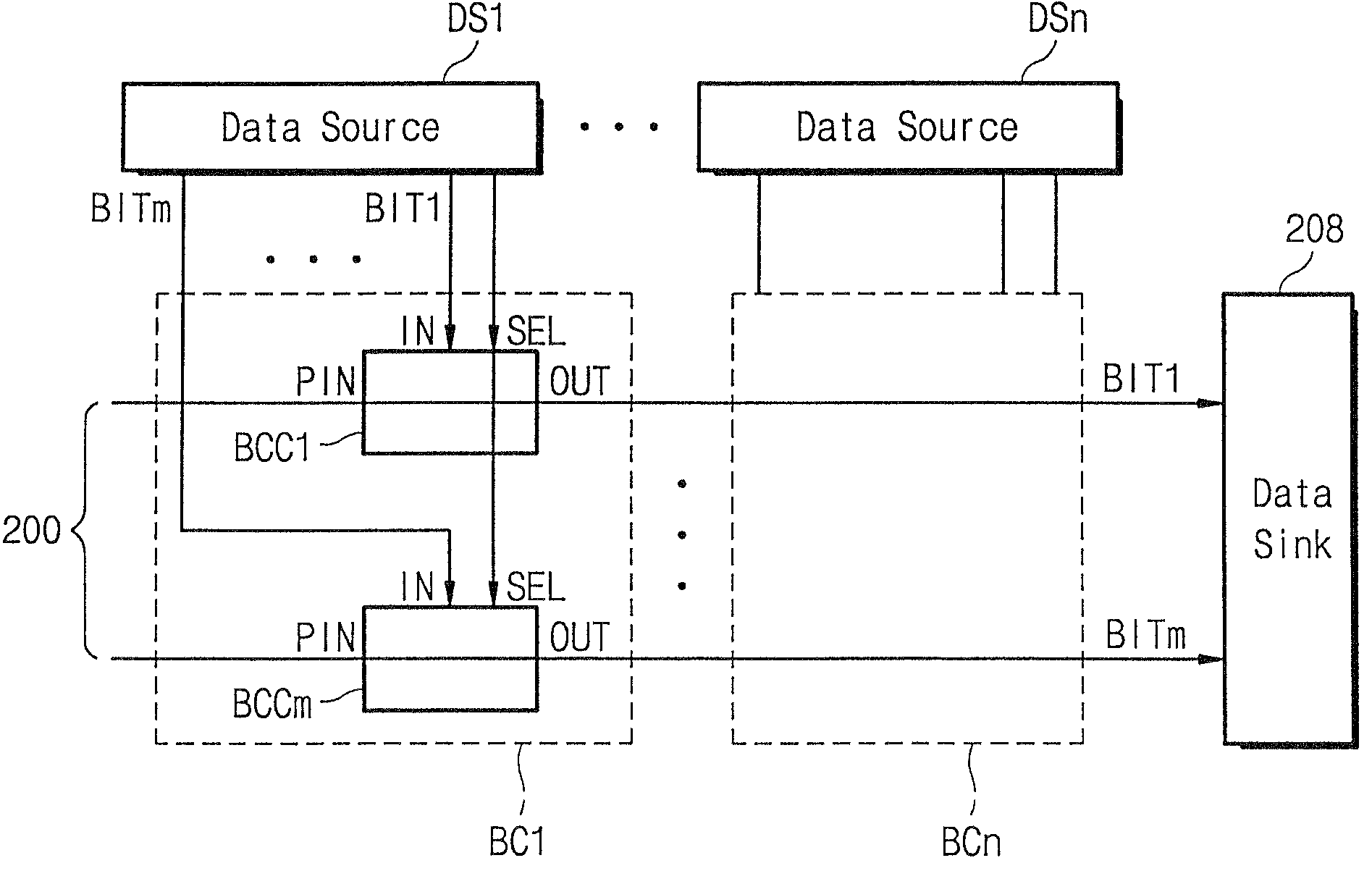
[0026]FIG. 2 shows a construction of a distributed bus system according to the invention, in which N data sources (DS1˜DSn) each generating M data bits (BIT0˜BITm) are connected to a bus 200. Bus cells BC1˜BCn have the same number as that of data sources DS1˜DSn. In other words, bus cells BC1-BCn and each has the same M-numbered bit connection circuit BCC1˜BCCm (only BCC1 is indicated), where M corresponds to the number of the data bits. The reference numerals IN, SEL, PIN, and OUT denote an input of the data bit from the data source, a selection signal determining selection for the data source corresponding thereto, an output from a prestage bit connection circuit, and an output of the bit connection circuit, respectively. The data bits BIT1˜BITm are coupled to the bit connection circuits BCC1˜BCCm together with the outputs PINs from the pre-stage bit connection circuits. The selection signals SELs, being generated from a bus controller (not shown) in the digital system employing t...

second embodiment

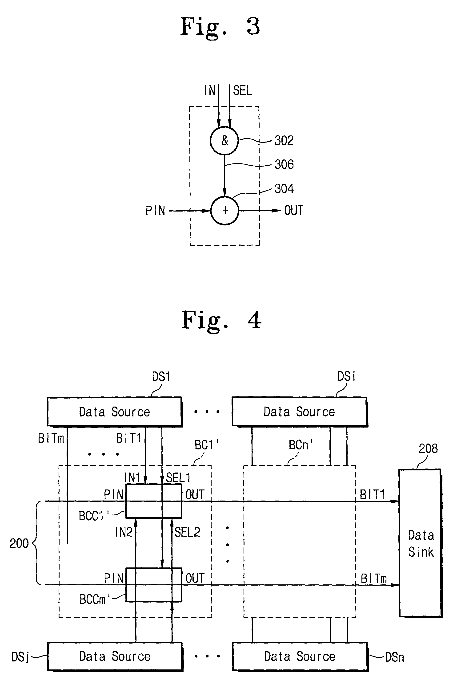
[0041]As shown in FIG. 6, each block chain may be constructed in the form of that shown in FIG. 4, i.e., one bus cell BC being assigned to two data sources (DSs). An OR gate 606 is disposed between the block chains, 602 and 604, and the data sink 208 to transfer a valid data bit to the data sink 208. The data bit output from the OR gate 606 is one provided from a selected data source and transferred through the bus cells including one that is interconnected to the selected data source, in one of the block chains 602 or 604. The OR gate 606 can be arranged for each data bit. The maximum value of delay time in the bus system shown in FIG. 6 is a sum of a delay time through the block chain and a delay time at the OR gate 606, approximately being one half of that of the second embodiment shown in FIG. 4.

[0042]As stated above, the invention offers useful techniques to reduce the number of interconnections from M*N to M, smaller than that with centralized single MUX-based buses and the sa...


PUM


Abstract

A bus system for providing a common data transmission path for N data sources that have M data bits. The N data sources are connected to M interconnections correspondingly through N bus cells each of which includes logic circuits for selectively providing the data bits of data sources into the interconnections. The bus cells are controlled to connect each of the data bits of the data sources to the selected one of the interconnections. The bus system is capable of adapting to delay times or loads of the data sources. The bus system reducing the number and the length of the interconnections.

Description

RELATED APPLICATION[0001]This application claims priority to Korean Patent Application No. 2001-20385, filed on Apr. 17, 2001, the contents of which are herein incorporated by reference in their entirety.FIELD OF THE INVENTION[0002]The present invention generally relates to distributed bus systems and, more specifically, to distributed bus systems adaptable to embedded system-on-a-chip (SOC).BACKGROUND OF THE INVENTION[0003]It is known in the art to employ a multiplicity of registers in a digital system. It is also known in the art to construct routes, in such a digital system for transferring data from one register to another register. A bus, which is an assemblage of common transmission lines controlled by switching circuits, has been utilized as a common route to efficiently perform data transmission between registers.[0004]Recently, some bus architectures for embedded SOCs are changing to ones that basically are associated with at least one multiplexer (or MUX), i.e., MUX-based ...

Claims


Application Information

Patent Timeline
Patent Type & Authority Patents(United States)
IPC IPC(8): H04L12/28G06F13/38G06F13/40
CPCG06F13/4068G06F13/38
Inventor CHOI, HOON
Owner SAMSUNG ELECTRONICS CO LTD
Why Eureka
Try Eureka