Memory systems, on-die termination (ODT) circuits, and method of ODT control

a memory system and on-die termination technology, applied in the field of memory systems, can solve problems such as degraded signal integrity, increased data rate, and signal integrity degraded in the memory system

Inactive Publication Date: 2010-08-31
SAMSUNG ELECTRONICS CO LTD
View PDF17 Cites 30 Cited by
  • Summary
  • Abstract
  • Description
  • Claims
  • Application Information

AI Technical Summary

Benefits of technology

[0014]According to still another aspect of the present invention, a memory system is provided which includes a data bus, a controller which generates a plurality clock enable signals and an plurality of on-die-termination (ODT) control signals, and a plurality of memory devices coupled to the data bus. Each of the memory devices includes an ODT circuit which is responsive to a respective clock enable signal and a respective ODT control signal to provide a resistive termination for the data bus. Further, the ODT circuit delays the transition from an asynchronous ODT circuit path to a synchronous ODT circuit path to compensate for an operational latency of a delay locked loop (DLL) circuit of the memory device.
[0015]According to yet another aspect of the present invention, a method of controlling an on-die termination (ODT) circuit during transition from a first power mode to a second power mode of a memory device is provided. The method includes delaying the transition from an asynchronous ODT circuit path to a synchronous ODT circuit path to compensate for an operational latency of a delay locked loop (DLL) circuit.

Problems solved by technology

Generally, as the bus frequency of a memory system (e.g., a memory system employing DRAM devices) increases, the signal integrity within the memory system degrades.
However, any increase in data rate beyond 300 Mbps tends to degrade signal integrity by increasing the load of the bus having the resistive stubs.
In fact, a data rate of 400 Mbps or greater is generally not achievable with the SSTL bus configuration.
However, a considerable amount of time is required to enable the active termination resistors installed in the DRAM circuits in response to the active termination control signals, and, for example, when a module-interleaved write / read operation is performed, this time lapse can result in data bobbles, thereby degrading memory system performance.
However, in the case where the DLL or PLL is deactivated during a power down or standby mode of a corresponding memory module, enabling / disabling of the active termination resistor cannot be controlled in this manner.

Method used


Image

  • Memory systems, on-die termination (ODT) circuits, and method of ODT control
  • Memory systems, on-die termination (ODT) circuits, and method of ODT control
  • Memory systems, on-die termination (ODT) circuits, and method of ODT control

Examples


Embodiment Construction

[0032]The present invention will now be described in detail by way of preferred, but non-limiting, embodiments of the invention. The embodiments are presented as examples only, and the invention is not considered to be limited to the specific configurations and / or features of the exemplary embodiments. Like elements are represented by like reference numbers throughout the drawings.

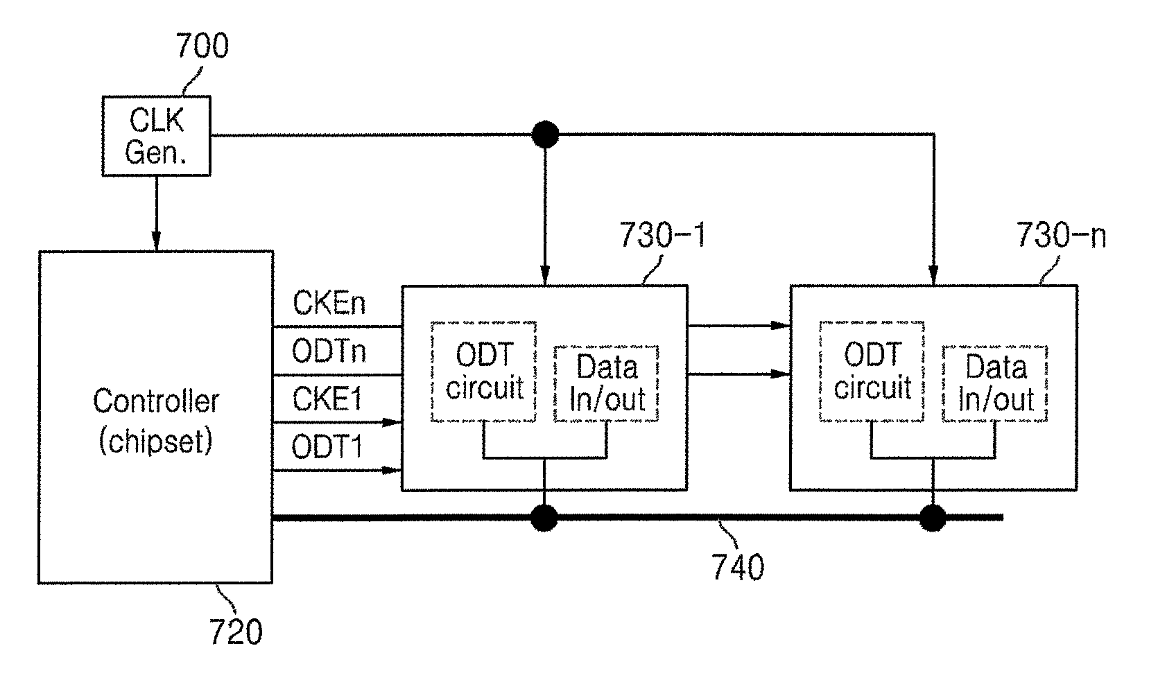
[0033]In commonly assigned U.S. Pat. No. 6,754,132, various on-die-termination (ODT) techniques are described.

[0034]The '132 patent describes, for example, an ODT control circuit having a synchronous transmission path and an asynchronous transmission path. Briefly, the synchronous path is utilized to process an externally supplied ODT control signal during an active / standby operational mode of the memory device, and the asynchronous path is utilized to process the externally supplied ODT control signal during a pre-charge power down operational mode of the memory device.

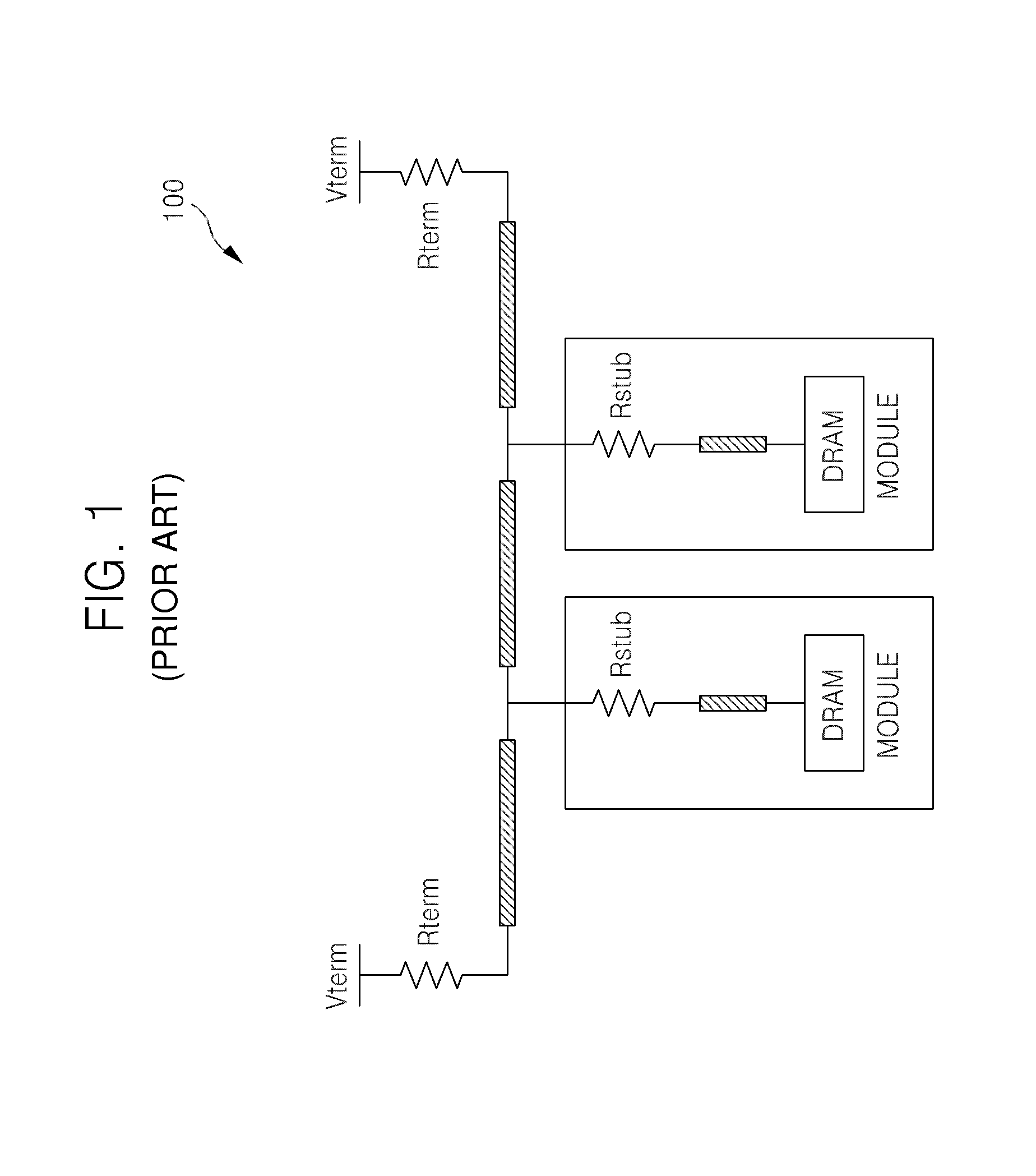
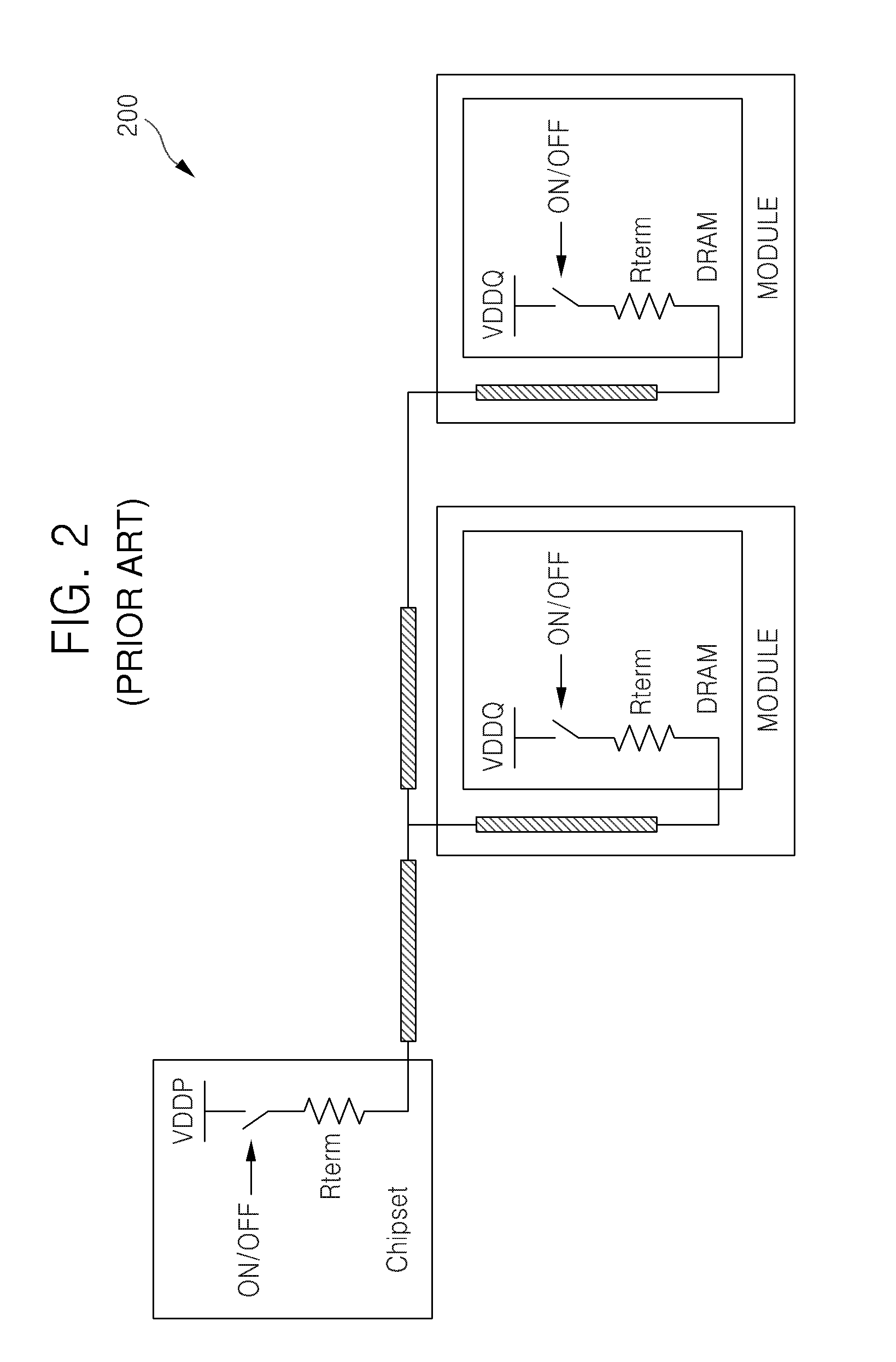
[0035]Memory devices, such as DDR (d...


PUM


Abstract

According to one aspect, an on-die termination (ODT) circuit is controlled during transition from a first power mode to a second power mode of a memory device. The transition from an asynchronous ODT circuit path to a synchronous ODT circuit path is delayed to compensate for an operational latency of a delay locked loop (DLL) circuit.

Description

BACKGROUND OF THE INVENTION[0001]1. Field of the Invention[0002]The present invention generally relates to memory circuits and systems, and more particularly, the present invention relates to memory systems utilizing on-die termination (ODT) schemes, to ODT circuits of memory systems, and to methods of ODT control.[0003]2. Description of the Related Art[0004]Generally, as the bus frequency of a memory system (e.g., a memory system employing DRAM devices) increases, the signal integrity within the memory system degrades. Thus, a variety of bus topologies capable of reducing signal distortion have been developed. For example, it is known that the use of resistive terminations at either the receiver and / or transmitter sides within the memory system is an effective means for absorbing reflections and thereby improving signal performance. Resistive termination configurations of this type generally fall into one of two categories, i.e., passive termination or active termination.[0005]FIG....

Claims


Application Information

Patent Timeline
Patent Type & Authority Patents(United States)
IPC IPC(8): H03K17/16H03K19/003
CPCG11C7/1051G11C7/1057H04L25/0278H04L25/0292G11C7/1063G11C7/22H03K19/017545
Inventor OH, REUMJUNG, DAE-HEE
Owner SAMSUNG ELECTRONICS CO LTD
Why Eureka
Try Eureka