Method of manufacturing substrate

a manufacturing method and substrate technology, applied in the direction of semiconductor devices, semiconductor/solid-state device details, electrical devices, etc., can solve the problem of not being able to meet the needs of the market,

Inactive Publication Date: 2010-09-14
SHINKO ELECTRIC IND CO LTD
View PDF4 Cites 28 Cited by
  • Summary
  • Abstract
  • Description
  • Claims
  • Application Information

AI Technical Summary

Benefits of technology

[0025]According to the present invention, the method includes: etching the silicon substrate from the first surface of the silicon substrate by the Bosch process in order to form the through hole; forming the thermal oxide film such that the thermal oxide film covers the first surface of the silicon substrate, the second surface of the silicon substrate opposite to the first surface, and the surface of the silicon substrate corresponding to the side surface of the through hole, by thermally oxidizing the silicon substrate where the through hole is formed; and removing the thermal oxide film. Accordingly, in the thermal oxide film forming step, all of the acicular protrusions made of silicon, which are formed when the through hole is formed, become a part of the thermal oxide film; and the thermally oxidized acicular protrusions can be removed together with the thermal oxide film in the thermal oxide film removing step. For this reason, since the defects are not formed on the insulating film formed on the surface of of the silicon substrate corresponding to the side surface of the through hole after the thermal oxide film removing step, it is possible to sufficiently ensure an insulating property between the silicon substrate and the through electrode by the insulating film.
[0027]According to the present invention, it is possible to form the through hole in a preferable shape without a notch. Furthermore, if the silicon substrate is ground in the thermal oxide film removing step, it is possible to remove the abrasive grains or the polishing chips, which adhere to the side surface of the through hole, together with the thermal oxide film. Therefore, since defects are not formed in the insulating film formed on the surface of the silicon substrate corresponding to the side surface of the through hole after the thermal oxide film removing step, it is possible to sufficiently ensure an insulating property between the silicon substrate and the through electrode by the insulating film.
[0029]According to the present invention, the method includes: etching the silicon substrate from the first surface of the silicon substrate by the Bosch process in order to form the through hole; removing the portion of the silicon substrate corresponding to the side surface of the through hole by wet etching; and forming the insulating film such that the insulating film covers the first and second surfaces of the silicon substrate and the surface of the silicon substrate corresponding to the side surface of the through hole. Accordingly, in the wet etching step, it is possible to remove the acicular protrusions made of silicon that are formed when the through hole is formed. Therefore, since defects are not formed in the insulating film formed on the surface of the silicon substrate corresponding to the side surface of the through hole after the wet etching step, it is possible to sufficiently ensure an insulating property between the silicon substrate and the through electrode by the insulating film.
[0031]According to the present invention, it is possible to form the through hole in a preferable shape without a notch. Furthermore, if the silicon substrate is ground in the wet etching step, it is possible to remove the abrasive grains or the polishing chips, which adhere to the side surface of the through hole, together with the portion of the silicon substrate corresponding to the side surface of the through hole.

Problems solved by technology

If the above-mentioned problem occurs, there has been a problem in that it is not possible to sufficiently ensure an insulating property between the silicon substrate 211 and the through electrode 213 by the insulating film 212 formed on the through hole 216.

Method used


Image

  • Method of manufacturing substrate
  • Method of manufacturing substrate
  • Method of manufacturing substrate

Examples


first embodiment

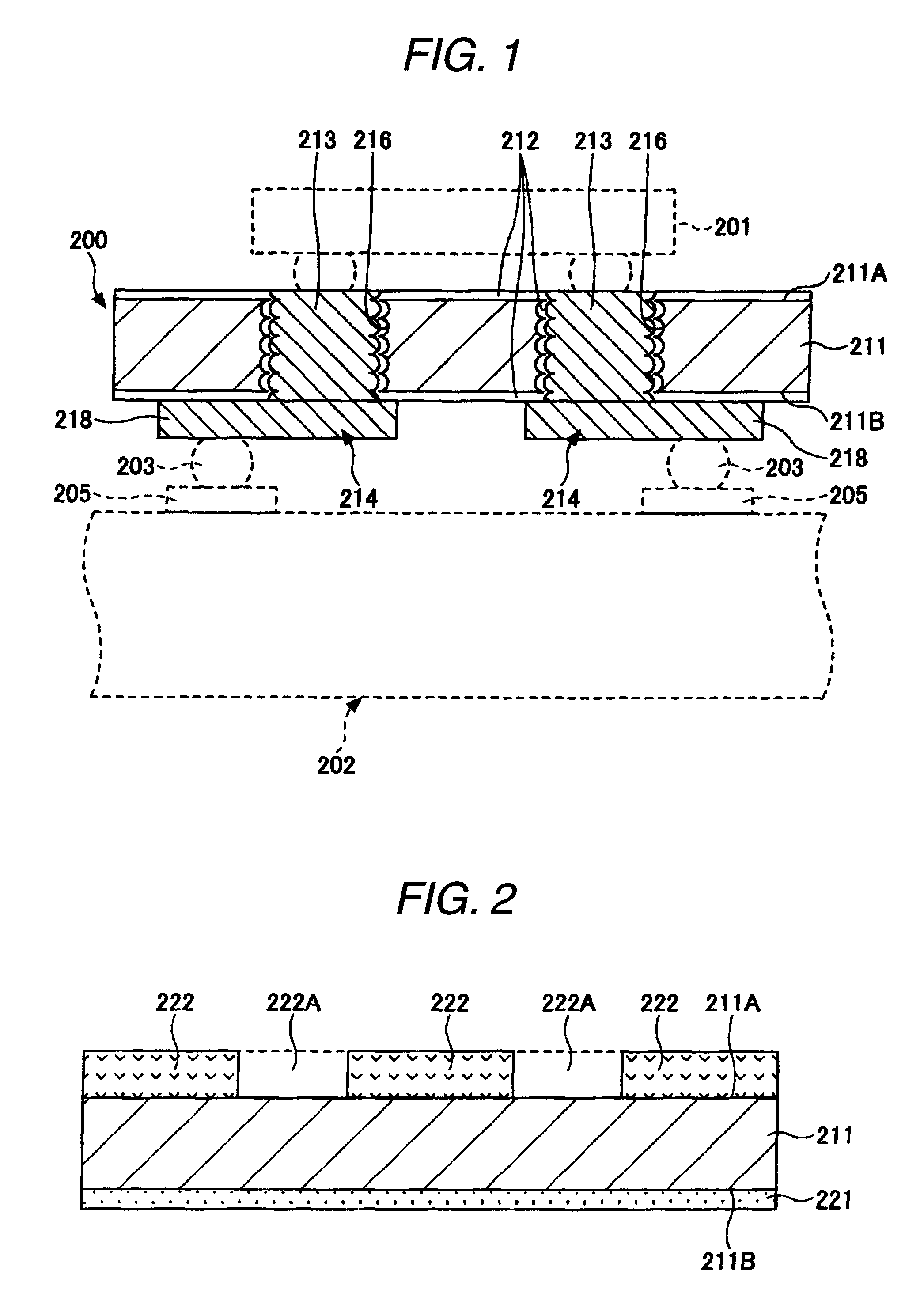
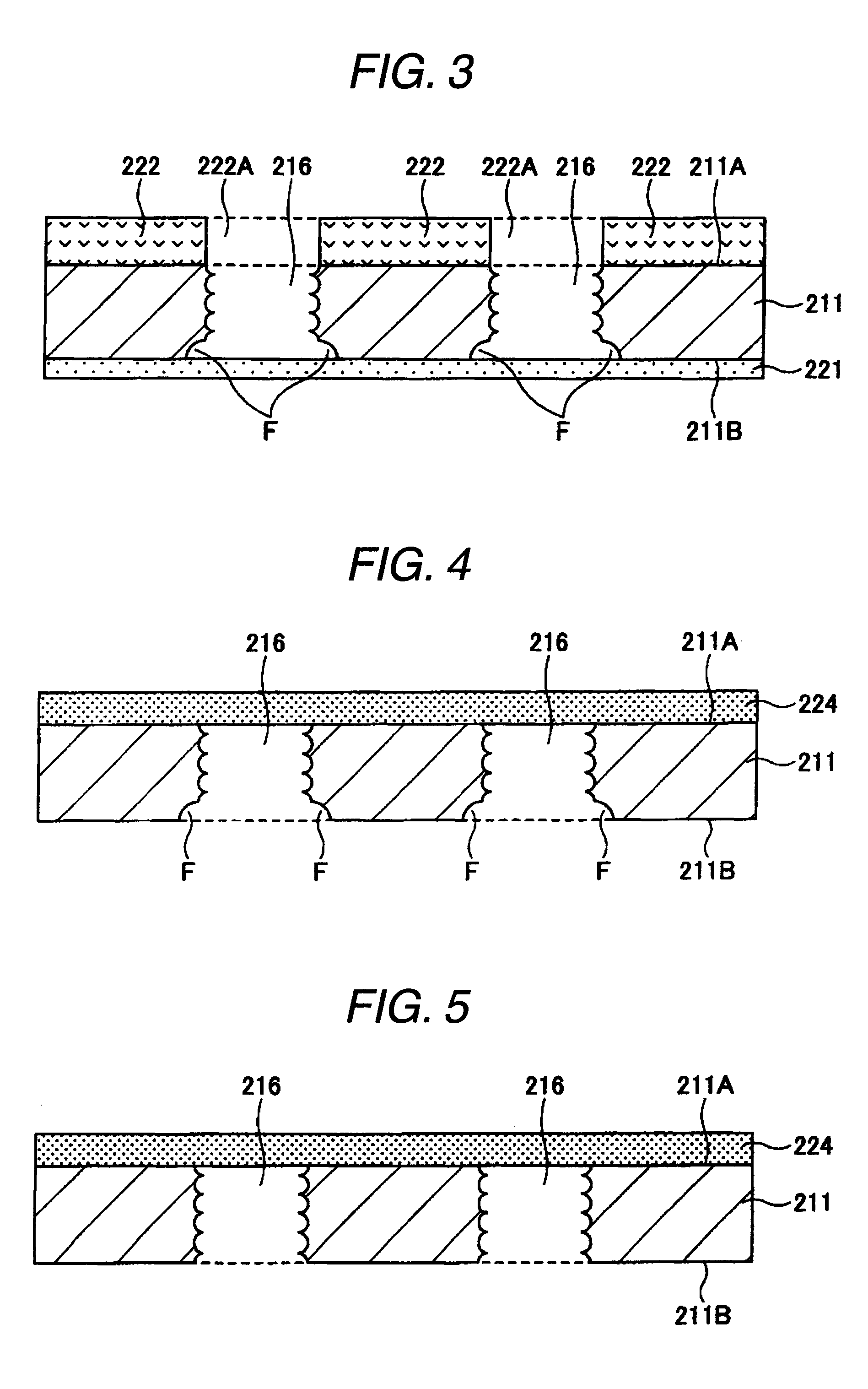
[0083]FIG. 11 is a cross-sectional view of a substrate according to a first embodiment of the invention.

[0084]Referring to FIG. 11, a substrate 10 includes a silicon substrate 21, an insulating film 22, a through electrode 23, and wiring 24. The silicon substrate 21 is formed into a plate shape, and includes a through hole 26. The through hole 26 is formed by a Bosch process. The Bosch process is a deep etching technique for silicon, specifically, an etching method of repeatedly performing etching (etching step) and etched sidewall protection (protecting step). Isotropic etching is performed using sulfur hexafluoride (SF6) in the etching step, and a sidewall is protected (etching performed in a transverse direction is controlled) using Teflon (registered trademark) gas (for example, C4F8) in the protecting step. Since the etching step and the protecting step are repeatedly performed in the Bosch process, the side surface of the through hole 26 formed by the Bosch process is formed i...

second embodiment

[0106]FIG. 24 is a cross-sectional view of a substrate according to a second embodiment of the present invention. In FIG. 24, the same components as those of the substrate 10 according to the first embodiment are represented by the same reference numerals.

[0107]Referring to FIG. 24, a substrate 50 according to a second embodiment has the same configuration as the substrate 10 except that a through hole 51 is formed instead of the through hole 26 formed in the substrate 10 according to the first embodiment.

[0108]The through hole 51 has the same configuration as the through hole 26 except that the scalloping shape of a portion of the silicon substrate 21 corresponding to the side surface of the through hole 51 is smoother than the scalloping shape of the portion of the silicon substrate 21 corresponding to the side surface of the through hole 26 formed in the substrate 10.

[0109]FIGS. 25 to 28 are views illustrating steps of manufacturing the substrate according to the second embodimen...
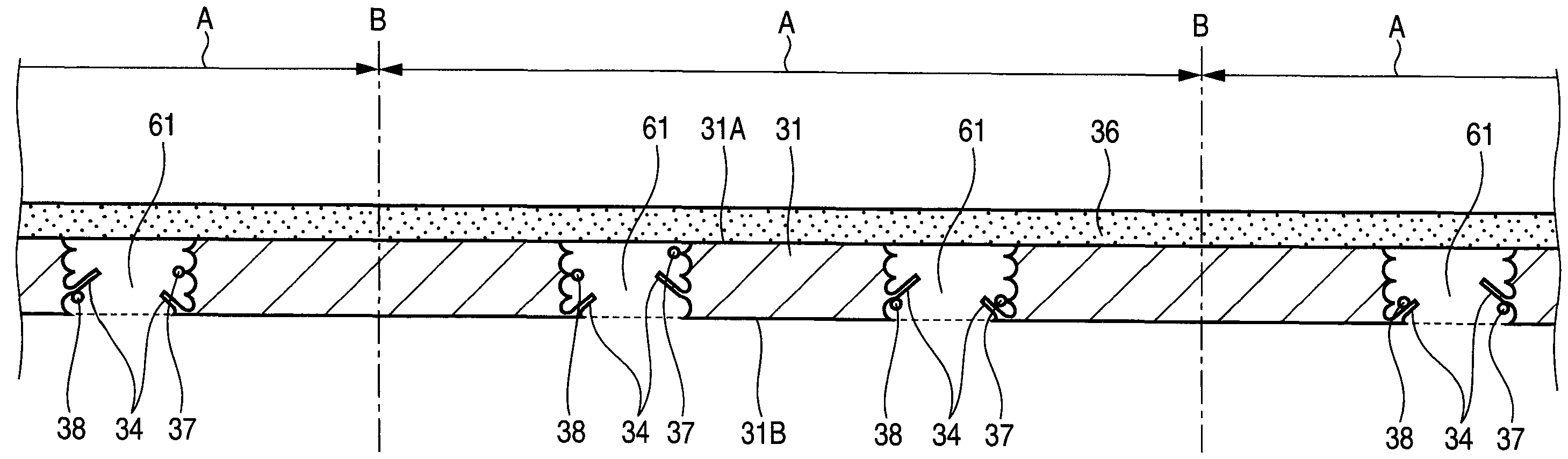
third embodiment

[0120]FIGS. 29 to 40 are views illustrating steps of manufacturing the substrate according to the third embodiment of the present invention. In FIGS. 29 to 40, the same components as those described in the steps of manufacturing the substrate according to the first embodiment are represented by the same reference numerals, and their description will be omitted hereinafter.

[0121]The steps of manufacturing the substrate in the third embodiment are different from those in the first embodiment in terms of formation step of the through hole. Specifically, the third embodiment is different from the first embodiment in that a hole 60 is formed in the silicon substrate 31 from the upper surface 31A of the silicon substrate 31, and then the silicon substrate 31 are ground from the lower surface 31B of the silicon substrate 31, so that the through hole is formed. Hereinafter, the steps of manufacturing the substrate in the third embodiment will be described with reference to FIGS. 29 to 40.

[0...


PUM

PropertyMeasurementUnit
thicknessaaaaaaaaaa
thicknessaaaaaaaaaa
diameteraaaaaaaaaa

Abstract

A method of manufacturing a substrate, includes: (a) forming the through hole by etching the silicon substrate from a first surface of the silicon substrate by a Bosch process; (b) forming a thermal oxide film such that the thermal oxide film covers the first surface of the silicon substrate, a second surface of the silicon substrate opposite to the first surface, and a surface of the silicon substrate corresponding to a side surface of the through hole, by thermally oxidizing the silicon substrate where the through hole is formed; (c) removing the thermal oxide film; (d) forming an insulating film such that the insulating film covers the first and second surfaces of the silicon substrate and the surface of the silicon substrate corresponding to the side surface of the through hole; and (e) forming the through electrode in the through hole on which the insulating film is formed.

Description

[0001]This application is based on and claims priority from Japanese Patent Application No. 2007-263224, filed on Oct. 9, 2007, the entire contents of which are hereby incorporated by reference.BACKGROUND[0002]1. Technical Field[0003]The present disclosure relates to a method of manufacturing a substrate that includes a through hole formed in a silicon substrate and a through electrode formed in the through hole and being insulated form the silicon substrate.[0004]2. Related Art[0005]In the past, a substrate (see FIG. 1), which includes a through hole formed in a silicon substrate and a through electrode formed in the through hole and being insulated form the silicon substrate, has been used as a substrate (interposer) that electrically connects a semiconductor device with a mounting substrate such as a mother board.[0006]FIG. 1 is a cross-sectional view of a substrate in the related art.[0007]Referring to FIG. 1, a related-art substrate 200 includes a silicon substrate 211, an insu...

Claims


Application Information

Patent Timeline
Patent Type & Authority Patents(United States)
IPC IPC(8): H01L21/44
CPCH01L21/486H01L21/76898H01L2224/16225H01L2924/18301H01L2924/15311H01L23/32
Inventor TAGUCHI, YUICHISHIRAISHI, AKINORISUNOHARA, MASAHIROMURAYAMA, KEISAKAGUCHI, HIDEAKIHIGASHI, MITSUTOSHI
Owner SHINKO ELECTRIC IND CO LTD
Why Eureka
Try Eureka