Misfet

a technology of mosfet and mosfet, which is applied in the field of mosfet, can solve the problems of deterioration of characteristics such as transconductance and high frequency response, peculiarity of known mosfet, and harmful effects on its characteristics as ideal mos devices, etc., and achieves excellent electronic characteristics, high breakdown voltage, and high speed operation.

Inactive Publication Date: 2003-12-11
PANASONIC CORP
View PDF5 Cites 45 Cited by
  • Summary
  • Abstract
  • Description
  • Claims
  • Application Information

AI Technical Summary

Benefits of technology

[0011] It is therefore an object of the present invention to ensure a high-speed operation and a high breakdown voltage in a semiconductor device with a MISFET structure provided on a compound semiconductor substrate. It is another object of this invention to provide a semiconductor device exhibiting excellent electronic characteristics by using means for preventing harmful effects on characteristics of a transistor resulting from interface states or fixed charges created between a gate insulating film and a channel region.

Problems solved by technology

In addition, the known MOSFET has problems peculiar to semiconductor devices including compound semiconductor layers.
Specifically, a lot of interface states and charges exist at the interface between the gate insulating film 104 and the doped channel SiC layer 102 in the known NMOSFET, thus causing harmful effects on its characteristics as an ideal MOS device.
Simultaneously, carriers (electrons) flowing through the channel are affected by interaction with the charges, resulting in decrease in channel mobility and deterioration in characteristics such as transconductance and high frequency response.
Likewise, in a PMOSFET, negative charges are trapped in a gate insulating film, resulting in deterioration in characteristics of the device.
In addition to the device using the SiC substrate, devices using a substrate made of a compound semiconductor such as GaAs or GaN also have the same problems.
At the present time, even if an oxide film formed on the surface of a compound semiconductor substrate is used as a gate insulating film, it is difficult for the device to obtain characteristics suitable for practical use.
Not only in the MOSFET but as long as an oxynitride film, a nitride film, or other metal oxide film (such as a tantalum oxide film) is used as a gate insulating film, the same problems might occur due to either positive or negative charge trapping.

Method used


Image

  • Misfet
  • Misfet
  • Misfet

Examples


example 2

[0132] A second example of experiment in which an active region, including .delta.-doped layers that exhibit a high electron mobility as shown in the first example, is used as a channel region of a MOSFET will be described.

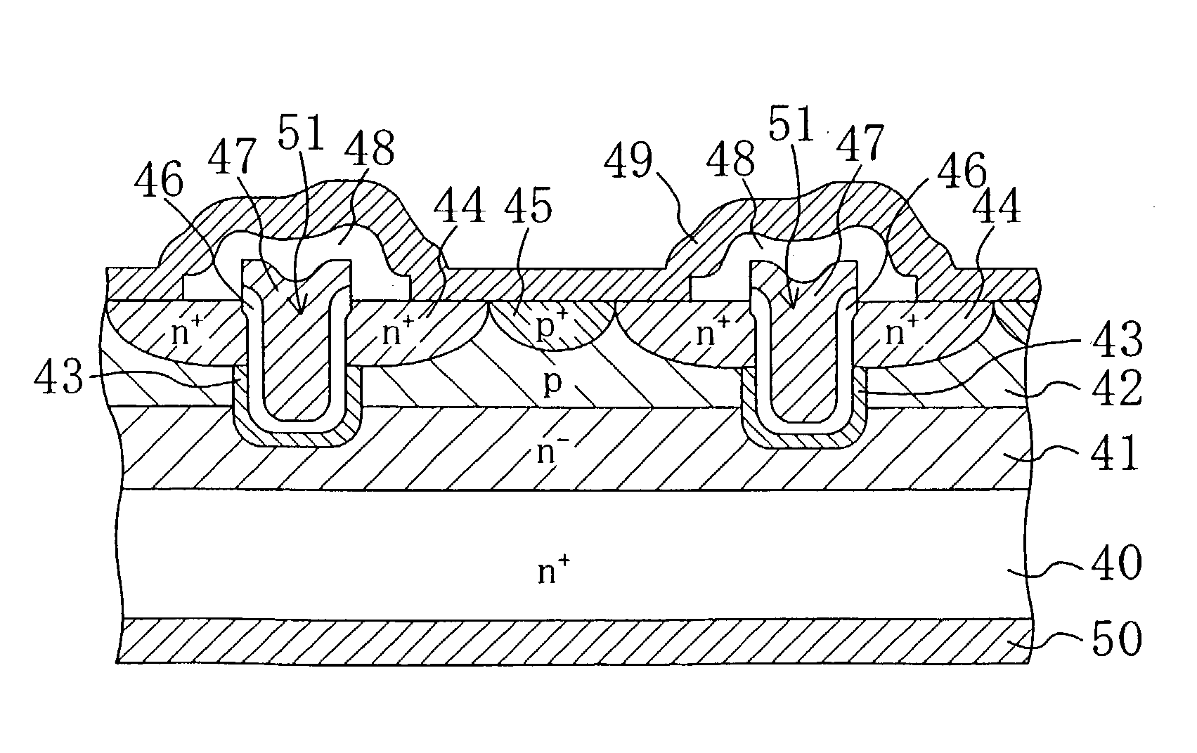
[0133] FIG. 21 shows cross-sectional views illustrating the structure of an ACCUFET according to this example. FIG. 21 shows p-type lower active region 61 doped with aluminum at a concentration of about 9.times.10.sup.15 atoms.multidot.cm.sup.-3 and formed on a p-type SiC substrate 60 doped with aluminum (a p-type impurity) at a concentration of 1.times.10.sup.18 atoms.multidot.cm.sup.-3; n-type upper active region 62 formed on the lower active region 61 and doped with nitrogen; n-type source / drain regions 63a and 63b formed by implanting nitrogen at a concentration of 1.times.10.sup.18 cm.sup.-3 into the upper and lower active regions 62 and 61; gate insulating film 64 of SiO.sub.2 formed on the upper active region 62; gate electrode 65 made of an Ni alloy film a...


PUM


Abstract

P-type active region 12; n-type source / drain regions 13a and 13b; gate insulating film 14 made of a thermal oxide film; gate electrode 15; source / drain electrodes 16a and 16b, are provided over a p-type SiC substrate 11. In the active region 12, p-type heavily doped layers 12a, which are thin enough to create a quantum effect, and thick undoped layers 12b are alternately stacked. When carriers flow, scattering of impurity ions in the active region is reduced, and the channel mobility increases. In the OFF state, a depletion layer expands throughout the active region, and the breakdown voltage increases. As a result of reduction in charges trapped in the gate insulating film or near the interface between the gate insulating film and the active region, the channel mobility further increases.

Description

[0001] The present invention relates to a MISFET formed by utilizing a compound semiconductor layer. More particularly, the present invention relates to a MISFET that has a high breakdown voltage and is suitable for use at a large current.[0002] Silicon carbide (SiC) is a semiconductor that has a wider bandgap than that of silicon (Si). Accordingly, SiC has a higher breakdown voltage and a higher melting point compared to Si. In view of these beneficial properties, SiC is a semiconductor material that is expected to be applied to next-generation power electronic devices, RF devices, high-temperature-operating devices and so on. It is also known that SiC can take various crystal structures including cubic ones such as 3C--SiC and hexagonal ones like 6H--SiC and 4H--SiC.[0003] FIG. 12 is a cross-sectional view schematically showing the structure of a known NMOS (Metal Oxide Semiconductor)-FET (Field Effect Transistor) that uses SiC. FIG. 12 shows p-type doped channel SiC layer 102 tha...

Claims


Application Information

Patent Timeline
Patent Type & Authority Applications(United States)
IPC IPC(8): H01L21/04H01L29/10H01L29/24H01L29/36H01L29/772H01L29/78
CPCH01L21/0455H01L29/105H01L29/1608H01L29/365H01L29/7828H01L29/7725H01L29/78H01L29/7813H01L29/7838H01L29/66068
Inventor YOKOGAWA, TOSHIYAKITABATAKE, MAKOTOKUSUMOTO, OSAMUTAKAHASHI, KUNIMASAUENOYAMA, TAKESHI
Owner PANASONIC CORP
Why Eureka
Try Eureka