Semiconductor device structure and methods of making

a technology of semiconductor devices and devices, applied in the direction of diodes, basic electric elements, electrical appliances, etc., can solve the problems of increasing the capacitance of the device, reducing the practical use of the device in the higher frequency circuit, and reducing the practical use of the device, so as to reduce the concentration of doping

Inactive Publication Date: 2011-09-01
HU JERRY +2
View PDF5 Cites 47 Cited by
  • Summary
  • Abstract
  • Description
  • Claims
  • Application Information

AI Technical Summary

Benefits of technology

[0017]It is an object of the present invention to find approaches to reduce the doping concent...

Problems solved by technology

In the prior art described in U.S. Pat. No. 6,867,436, it is inherently difficult to construct the device that achieves a device capacitance sufficiently low for any practical utilization in higher frequency circuit.
This translates unfavorably into increased device cap...

Method used


Image

  • Semiconductor device structure and methods of making
  • Semiconductor device structure and methods of making
  • Semiconductor device structure and methods of making

Examples


embodiment

of FIG. 4

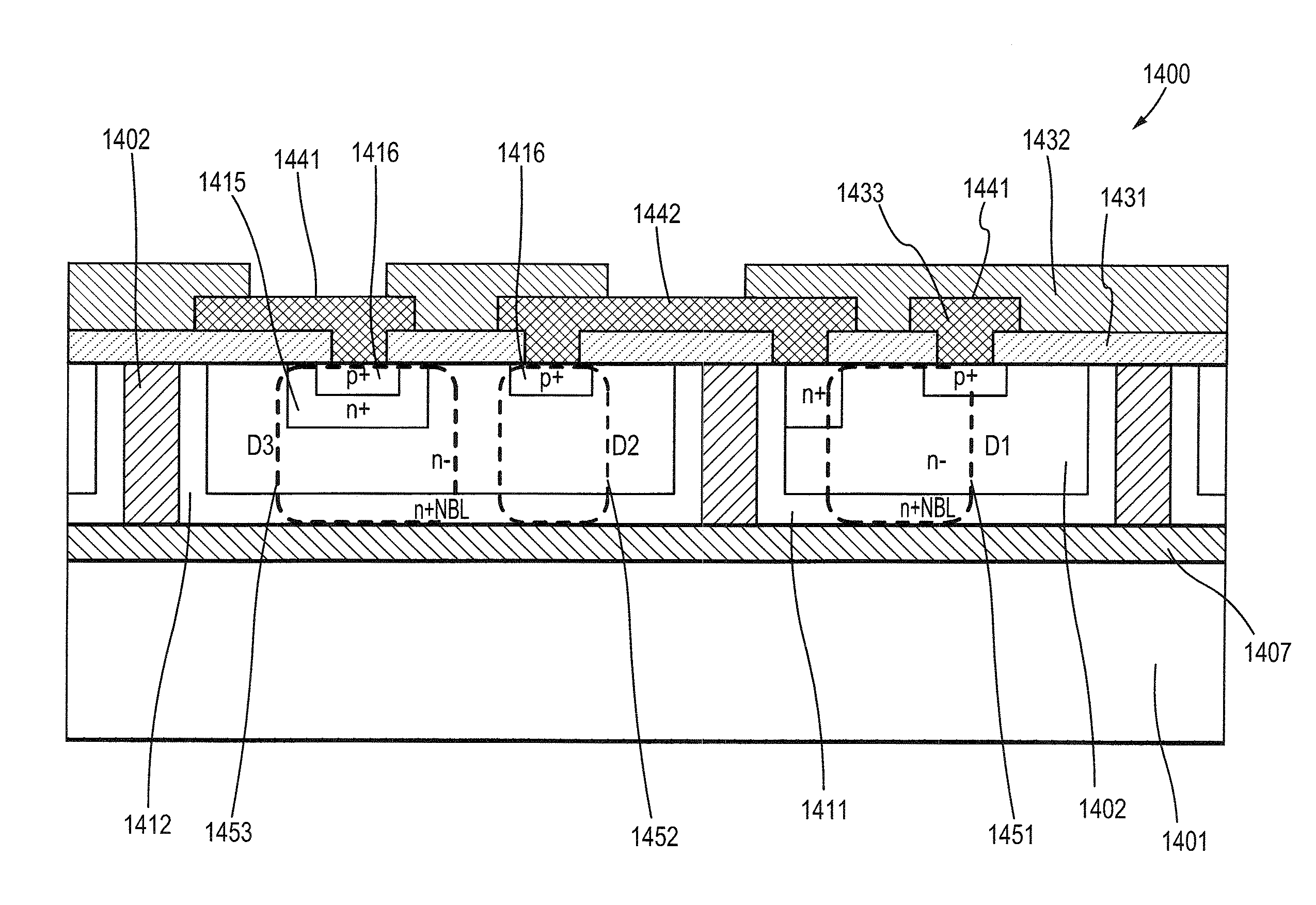
[0078]Though the main semiconductor device component for protection purpose in a typical, unidirectional or bidirectional, assembled device is a conventional unidirectional diode, however, it can be constructed of a diode, a transistor, a thyristor, an assembled device, or a circuit that functions the same as a conventional unidirectional or bidirectional transient voltage suppressing and electrostatic discharge protection device.

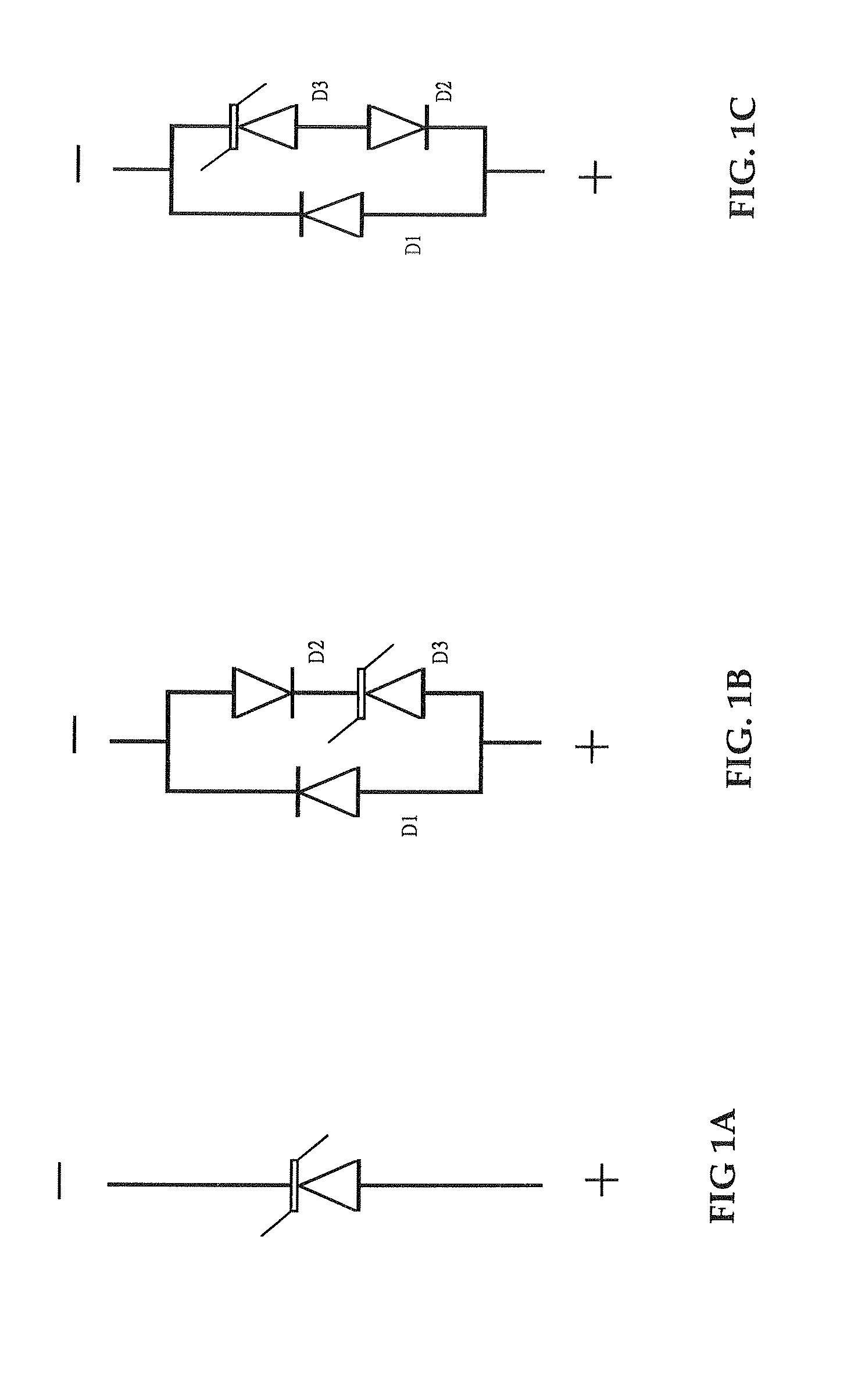
[0079]FIG. 4 is a cross-sectional view illustrating the semiconductor construction of a unidirectional assembled device of the present invention. The device 400 is fabricated in accordance with a preferred embodiment of the present invention. Equivalent circuit of the unidirectional assembled device 400 is the same as that shown in FIG. 1B.

[0080]The unidirectional assembled device 400 comprises a p-type semiconductor substrate, or substrate 401. An n+ buried layer (NBL) 411 is disposed on the substrate surface 405, and an n− epitaxial layer 402 is ...


PUM


Abstract

A process for fabricating a semiconductor device having reduced capacitance for high frequency circuit protection is disclosed that comprises first forming an n+ buried layer in a p-type substrate by depositing n-type dopant on the top surface of the substrate and then drive in or by implanting n-type material into the substrate, and then growing an n-type epitaxial layer atop the n+ buried layer as the device layer. Trenches that surrounds the device region with depth extending from the top surface, going through the n+ buried layer and reaching down to the substrate are then formed and then an n+ layer on the sidewalls of the trenches is formed by diffusion or ion implantation. The trenches are then filled by growing a layer of thermal oxide on the sidewalls of the trenches and followed by deposition of plasma enhanced oxide, nitride, TEOS oxide CVD oxide, or polysilicon into the trenches and then planarizing the top surface by plasma etch back or polishing. Then n+ region of the device is formed by forming an oxide layer on the top surface of the device layer and then etching the oxide by photolithography, then depositing n-type dopant material and then driving in by high temperature diffusion. Finally p+ region of the device is formed by etching the oxide using photolithography, then depositing p-type dopant material by solid or gas phase deposition or ion implantation and then driving in by high temperature diffusion so that the breakdown voltage between cathode and anode of the device is set to a targeted voltage for high frequency circuit protection.

Description

BACKGROUND OF THE INVENTION[0001]1. Field of the Invention[0002]The present invention relates in general to semiconductor devices and more particularly to semiconductor devices having reduced capacitance for protecting high frequency circuit applications from electrostatic discharge surge energy and transient electrical overstress.[0003]2. Description of Related Art[0004]In order to protect vulnerable circuits from electrical overstress such as that caused by electrostatic discharge, inductive load switching and lightning, a semiconductor device is usually employed to clamp the transient voltage to a nondestructive level. The semiconductor device for such transient voltage suppression purpose can be a diode, a transistor, a thyristor, an assembled device or a circuit.[0005]Conventionally, a unidirectional protection device for such application is a Zener or avalanche diode constructed out of a semiconductor p-n junction (FIG. 1A). Based on semiconductor physics, the depletion-layer ...

Claims


Application Information

Patent Timeline
IPC IPC(8): H01L21/762
CPCH01L21/761H01L21/76237H01L27/0817H01L27/0255H01L27/0814H01L21/76283
Inventor HU, JERRYLIN, PANCHIENHUANG, BERT
Owner HU JERRY
Why Eureka
Try Eureka