Silicon carbide for crystalline silicon solar cell surface passivation

a technology of silicon carbide and solar cell, which is applied in the manufacture of semiconductor/solid-state devices, electrical equipment, semiconductor devices, etc., can solve problems such as reducing the efficiency of solar cells, and achieve the effect of improving minority carrier lifetime measuremen

Inactive Publication Date: 2009-10-08
APPLIED MATERIALS INC
View PDF16 Cites 60 Cited by
  • Summary
  • Abstract
  • Description
  • Claims
  • Application Information

AI Technical Summary

Benefits of technology

[0009]Embodiments of the invention also provide methods for depositing a silicon carbide / silicon oxide passivation layer that acts as a high-quality surface passivation layer for solar cells. Since the silicon oxide forms a high internal reflection interface with conductive materials, higher reflection from the back surface of the solar cell increases the optical path of long wavelength light.

Problems solved by technology

The back contact is generally not constrained to be formed in multiple thin metal lines, since it does not prevent incident light from striking solar cell.
Each time an electron-hole pair recombines in a solar cell, charge carriers are eliminated, thereby reducing the efficiency of the solar cell.

Method used


Image

  • Silicon carbide for crystalline silicon solar cell surface passivation
  • Silicon carbide for crystalline silicon solar cell surface passivation
  • Silicon carbide for crystalline silicon solar cell surface passivation

Examples


Embodiment Construction

[0023]Embodiments of the present invention generally provide methods for depositing a silicon carbide (SiC) passivation layer that may act as a high-quality passivation layer for solar cells.

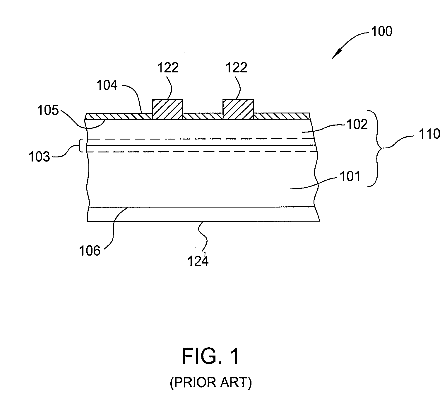
[0024]FIG. 1 schematically depicts a standard silicon solar cell 100 fabricated on a wafer 110. The wafer 110 includes base region 101, which is typically composed of p-type silicon, an emitter region 102, which is typically composed of n-type silicon, a p-n junction region 103 disposed therebetween, and a dielectric layer 104. P-n junction region 103 is disposed between base region 101 and emitter region 102 of the solar cell, and is the region in which electron-hole pairs are generated when solar cell 100 is illuminated by incident photons. Dielectric layer 104 acts as an anti-reflective coating (ARC) layer for solar cell 100 as well as a passivation layer for the surface 105 of emitter region 102.

[0025]When light falls on the solar cell, energy from the incident photons generates electron-hol...


PUM

PropertyMeasurementUnit
thicknessaaaaaaaaaa
thicknessaaaaaaaaaa
thicknessaaaaaaaaaa

Abstract

Embodiments of the present invention generally provide methods for depositing a silicon carbide (SiC) passivation layer that may act as a high-quality passivation layer for solar cells. Embodiments of the invention also provide methods for depositing a silicon carbide / silicon oxide passivation layer that acts as a high-quality rear surface passivation layer for solar cells. The methods described herein enable the use of deposition systems configured for processing large-area substrates for solar cell processing. According to embodiments of the invention, a SiC passivation layer may be formed with improved minority carrier lifetime measurements. The SiC passivation layer may be formed at a temperature between about 150° C. and 450° C., which is much lower than temperatures for thermal oxide passivation.

Description

CROSS-REFERENCE TO RELATED APPLICATIONS[0001]This application claims benefit of U.S. Provisional Patent Application Ser. No. 61 / 041,851, filed Apr. 2, 2008, which is herein incorporated by reference.BACKGROUND[0002]1. Field[0003]Embodiments of the present invention generally relate to the fabrication of solar cells and particularly to the rear surface passivation of crystalline silicon solar cells.[0004]2. Description of the Related Art[0005]Solar cells are photovoltaic devices that convert sunlight directly into electrical power. The most common solar cell material is silicon (Si), which is in the form of single or multi-crystalline wafers. Because the cost of electricity generated using silicon-based solar cells is higher than the cost of electricity generated by traditional methods, there has been an effort to reduce the cost of manufacturing solar cells that does not adversely affect the overall efficiency of the solar cell.[0006]When light falls on the solar cell, energy from t...

Claims


Application Information

Patent Timeline
Patent Type & Authority Applications(United States)
IPC IPC(8): H01L31/0224H01L31/18
CPCH01L31/02167Y02E10/50H01L31/18H01L31/022425
Inventor ZHOU, LISONGDIXIT, SANGEETA
Owner APPLIED MATERIALS INC
Why Eureka
Try Eureka