Organic electro-luminescence display device

a technology of electroluminescence display device and organic el, which is applied in the direction of discharge tube luminescnet screen, discharge tube/lamp details, organic semiconductor device, etc., can solve the problems of increasing the manufacturing cost of insufficient moisture capture effect, so as to prevent the reduction of light emission efficiency in the top-emission organic el display device. , the effect of simple process

Active Publication Date: 2010-09-28
SAMSUNG DISPLAY CO LTD +1
View PDF5 Cites 3 Cited by
  • Summary
  • Abstract
  • Description
  • Claims
  • Application Information

AI Technical Summary

Benefits of technology

[0012]An advantage of the present invention is that, with a simple process, reduction in light emission efficiency in the top-emission organic EL display device is prevented, moisture in the organic EL display device is captured, and generation or growth of a dark spot is inhibited.
[0013]The present invention is conceived in view of the above-described circumstances, and uses, as the desiccant of the organic EL display device, a desiccant comprising a material which is identical to the material which forms an electron transporting layer and comprising a co-evaporation layer having a greater composition of an alkali metal or an alkaline earth metal than the electron transporting layer. A characteristic of the present invention is that the desiccant comprising the co-evaporation layer is placed without overlapping the light emitting layer. More specifically, according to various aspects of the present invention, the following structures are provided.
[0014](1) According to one aspect of the present invention, there is provided a top-emission organic electro-luminescence display device in which an element substrate having a display region in which pixels each having an organic electro-luminescence layer sandwiched between an upper electrode and a lower electrode are formed in a matrix form is sealed by a sealing substrate and an image is formed on a side of the sealing substrate, wherein the organic electro-luminescence layer comprises an electron transporting layer, a light emitting layer, and a hole transporting layer, wherein the electron transporting layer is formed through co-evaporation of an organic material and an alkali metal or an alkaline earth metal, and a desiccant which comprises a material identical to the material of the electron transporting layer and comprises a co-evaporation layer having a greater composition ratio of the alkali metal or the alkaline earth metal than the electron transporting layer is placed without overlapping the light emitting layer.
[0015](2) According to another aspect of the present invention, it is preferable that, in the top-emission organic electro-luminescence display device of (1), the composition ratio of the alkali metal or the alkaline earth metal in the desiccant comprising the co-evaporation layer is greater than the composition ratio of the alkali metal or the alkaline earth metal in the electron transporting layer by greater than or equal to 50%.
[0016](3) According to another aspect of the present invention, there is provided a top-emission organic electro-luminescence display device in which an element substrate having a display region in which pixels each having an organic electro-luminescence layer sandwiched between an upper electrode and a lower electrode are formed in a matrix form is sealed by a sealing substrate and an image is formed on a side of the sealing substrate, wherein the organic electro-luminescence layer comprises an electron transporting layer, a light emitting layer, and a hole transporting layer, wherein the electron transporting layer is formed through co-evaporation of an organic material and cesium, and a desiccant which comprises a material identical to the material of the electron transporting layer and comprises a co-evaporation layer having a greater composition ratio of cesium than the electron transporting layer is placed without overlapping the light emitting layer.
[0017](4) According to another aspect of the present invention, it is preferable that, in the top-emission organic electro-luminescence display device of (3), the composition ratio of cesium in the desiccant comprising the co-evaporation layer is greater than the composition ratio of cesium in the electron transporting layer by greater than or equal to 50%.

Problems solved by technology

These steps increase the manufacturing cost of the organic EL display device.
In addition, with the composition identical to that of the organic EL layer, the moisture capturing effect may not be sufficient.

Method used


Image

  • Organic electro-luminescence display device
  • Organic electro-luminescence display device
  • Organic electro-luminescence display device

Examples


first preferred embodiment

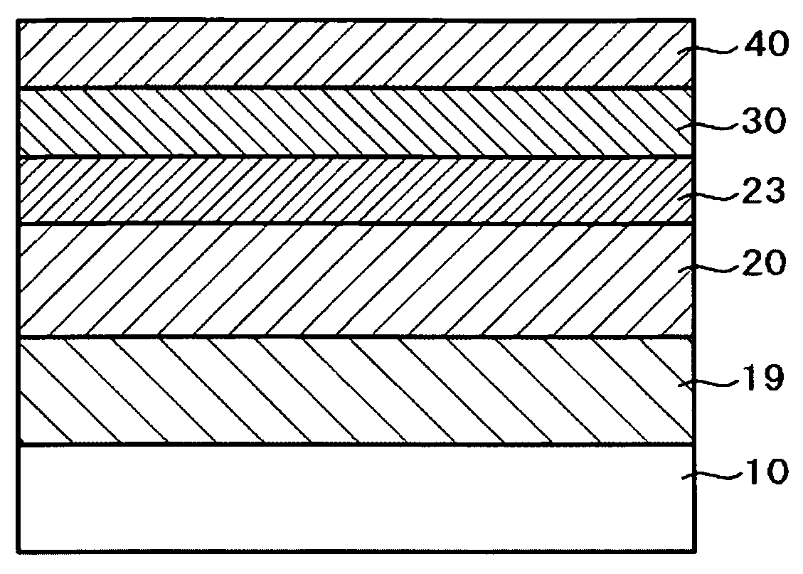
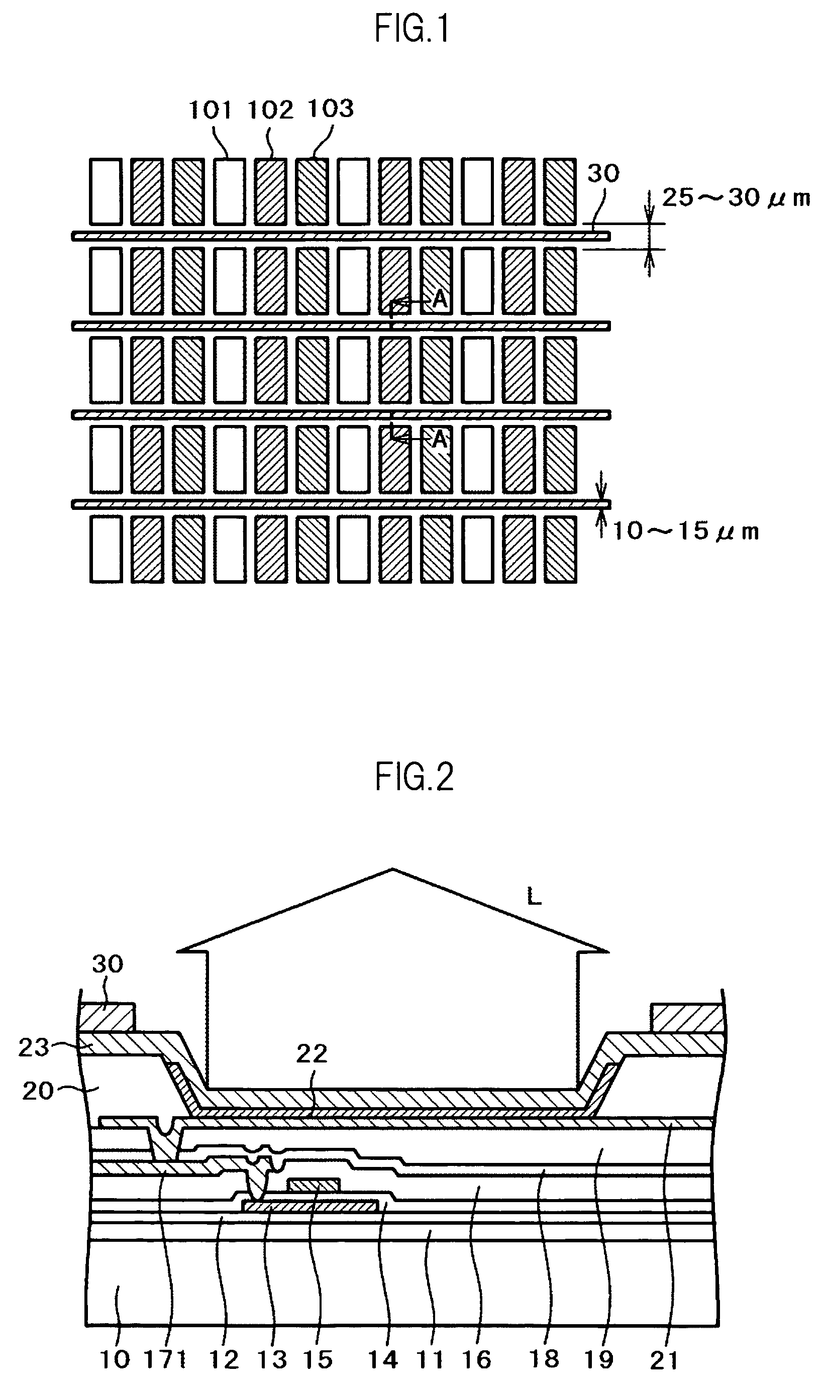
[0064]FIG. 4 is a cross sectional schematic view showing a first preferred embodiment of the present invention. In FIG. 4, the organic passivation film 19 is formed over the element substrate 10 comprising glass. The TFT, gate insulating film, interlayer insulating film, etc. which are formed below the organic passivation film 19 are not shown. The upper electrode 23 which functions as the anode is formed with IZO over the organic passivation film 19. The organic EL layer, lower electrode, etc. below the upper electrode 23 are not shown.

[0065]In the present embodiment, over the organic passivation film 19 in an area in which the upper electrode 23 is not present, a structure which uses the same materials as the electron transporting layer and has different constituent component is co-evaporated and is used as the desiccant 40. More specifically, the material is co-evaporation of an organic material and cesium as described above. As the desiccant 40, the composition of cesium is set ...

second preferred embodiment

[0071]FIG. 5 is a cross sectional schematic view showing a second preferred embodiment of the present invention. In FIG. 5, the organic passivation film 19 is formed over the element substrate 10 comprising glass. The elements formed below the organic passivation film 19 such as the TFT, gate insulating film, and interlayer insulating film are not shown. The upper electrode 23 which functions as the anode is formed with IZO over the organic passivation film 19. The elements below the upper electrode 23 such as the organic EL layer and the lower electrode are not shown.

[0072]In the present embodiment, the desiccant 40 by co-evaporation is formed over the upper electrode 23 in a region where the organic EL layer 22 is not present. Unlike the organic EL layer 22, the upper electrode 23 is evaporated in a pattern (so-called beta pattern) covering the entire surface of the element substrate 10 except for the terminal portion or the like. Therefore, the region where the upper electrode 23...

third preferred embodiment

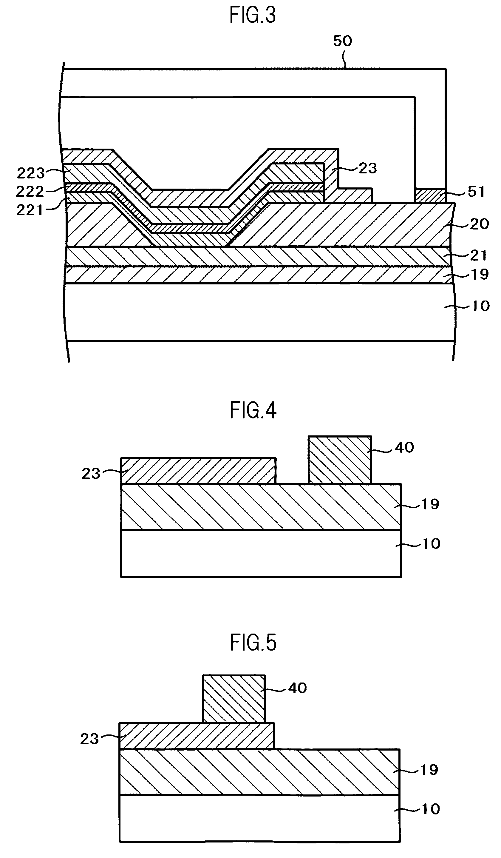
[0074]FIG. 6 is a cross sectional schematic view of a third preferred embodiment of the present invention. In FIG. 6, the organic passivation film 19 is formed over the element substrate 10 comprising glass. The elements formed below the organic passivation film 19 such as the TFT, gate insulating film, and interlayer insulating film are not shown. The bank 20 for separating the pixels is formed with an acrylic resin over the organic passivation film 19. The upper electrode 23 by IZO extends over the bank 20.

[0075]In the present embodiment, both the upper electrode 23 and the bank 20 are covered with the desiccant 40 deposited by co-evaporation. The acrylic resin forming the bank 20 has a characteristic that it easily contains moisture. The moisture contained in the acrylic resin is released during a long-term operation of the organic EL display device and reduces the light emission efficiency of the organic EL layer 22, resulting in a black spot or the like.

[0076]In the present emb...


PUM


Abstract

An organic electro-luminescence display device emits light by applying a voltage by an image signal between an upper electrode (23) and a lower electrode which sandwich an organic electro-luminescence layer. The organic electro-luminescence layer comprises an electron transporting layer, a light emitting layer, and a hole transporting layer. The electron transporting layer includes an organic material and cesium, and has a moisture absorbing characteristic. A structure in which the same materials as the electron transporting layer are used and which has a different constituent composition and a greater amount of cesium is used as a desiccant (40) and placed in a region which does not overlap the organic electro-luminescence layer, to effectively remove moisture inside the organic electro-luminescence display device.

Description

CROSS-REFERENCE TO RELATED APPLICATION[0001]The present application claims priority from Japanese application JP 2007-283708 filed on Oct. 31, 2007, the content of which is hereby incorporated by reference into this application.BACKGROUND OF THE INVENTION[0002]1. Field of the Invention[0003]The present invention relates to an organic electro-luminescence (hereinafter simply referred to as “EL”) display device, and, in particular, to a top-emission type organic EL display device in which generation of dark spots by moisture is inhibited and which is highly reliable.[0004]2. Description of the Related Art[0005]Organic EL display devices include a bottom-emission type in which light emitted from an organic EL layer is emitted in a direction toward a glass substrate over which the organic EL layer or the like is formed and a top-emission type in which the light emitted from the organic EL layer is emitted in a direction opposite to that toward the glass substrate over which the organic ...

Claims


Application Information

Patent Timeline
Patent Type & Authority Patents(United States)
IPC IPC(8): H05B33/00
CPCH01L51/5237H01L27/3244H01L2251/5315H10K59/122H10K50/16H10K50/814H10K50/824H10K50/846H10K2102/3026H01L2924/01055H10K59/12H10K50/15H10K50/11H10K50/84
Inventor TOYODA, HIRONORIMURAKAMI, HAJIMEKATO, SHINICHITANAKA, MASAHIRO
Owner SAMSUNG DISPLAY CO LTD
Why Eureka
Try Eureka