Memory construction apparatus for forming logical memory space

a technology of logical memory space and memory construction, applied in the field of memory construction apparatus, can solve the problems of increasing tat, difficult to select from devices, and limited in the number of usable physical rams and usable ffs, and achieve the effect of efficiently designing an integrated circui

Inactive Publication Date: 2010-09-28
FUJITSU LTD
View PDF3 Cites 2 Cited by
  • Summary
  • Abstract
  • Description
  • Claims
  • Application Information

AI Technical Summary

Benefits of technology

[0012]The present invention has been made in view of these problems, and an object thereof is to provide a memory construction apparatus for automatically forming a desired logical memory space, thereby making it possible to design an integrated circuit efficiently.

Problems solved by technology

However, there is an upper limit to the capacity of the memory which can be produced with the memory compiler by the conventional ASIC-developing technique, and therefore when the capacity of a logically required memory exceeds the upper limit, it is necessary to produce a circuit of a logical memory by combining several physical RAMs produced by the memory compiler and perform circuit debugging (using logic simulation), which causes an increase in TAT (Turn Around Time: a time period taken to perform a sequence of processes).
Further, it is difficult to predict how many physical RAMs are required at the beginning of design, and hence it is difficult to select from devices, such as an FPGA (Field Programmable Gate Array), a PLD (Programmable Logic Device), and a Structured ASIC, which are limited in the numbers of usable physical RAMs and usable FFs.
This can eventually cause the number of physical RAMs to exceed the limited number of usable RAMs, which compels a change in the combination of RAMs (change in the circuit), and further in the worst case, a change in the device.

Method used


Image

  • Memory construction apparatus for forming logical memory space
  • Memory construction apparatus for forming logical memory space
  • Memory construction apparatus for forming logical memory space

Examples


Embodiment Construction

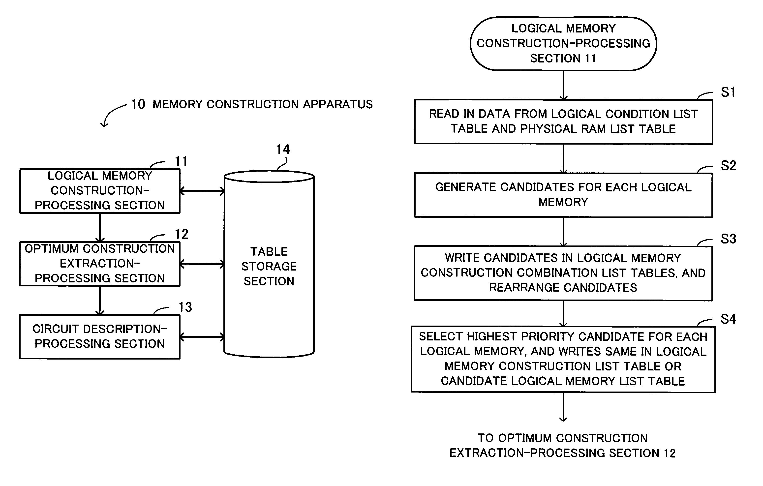
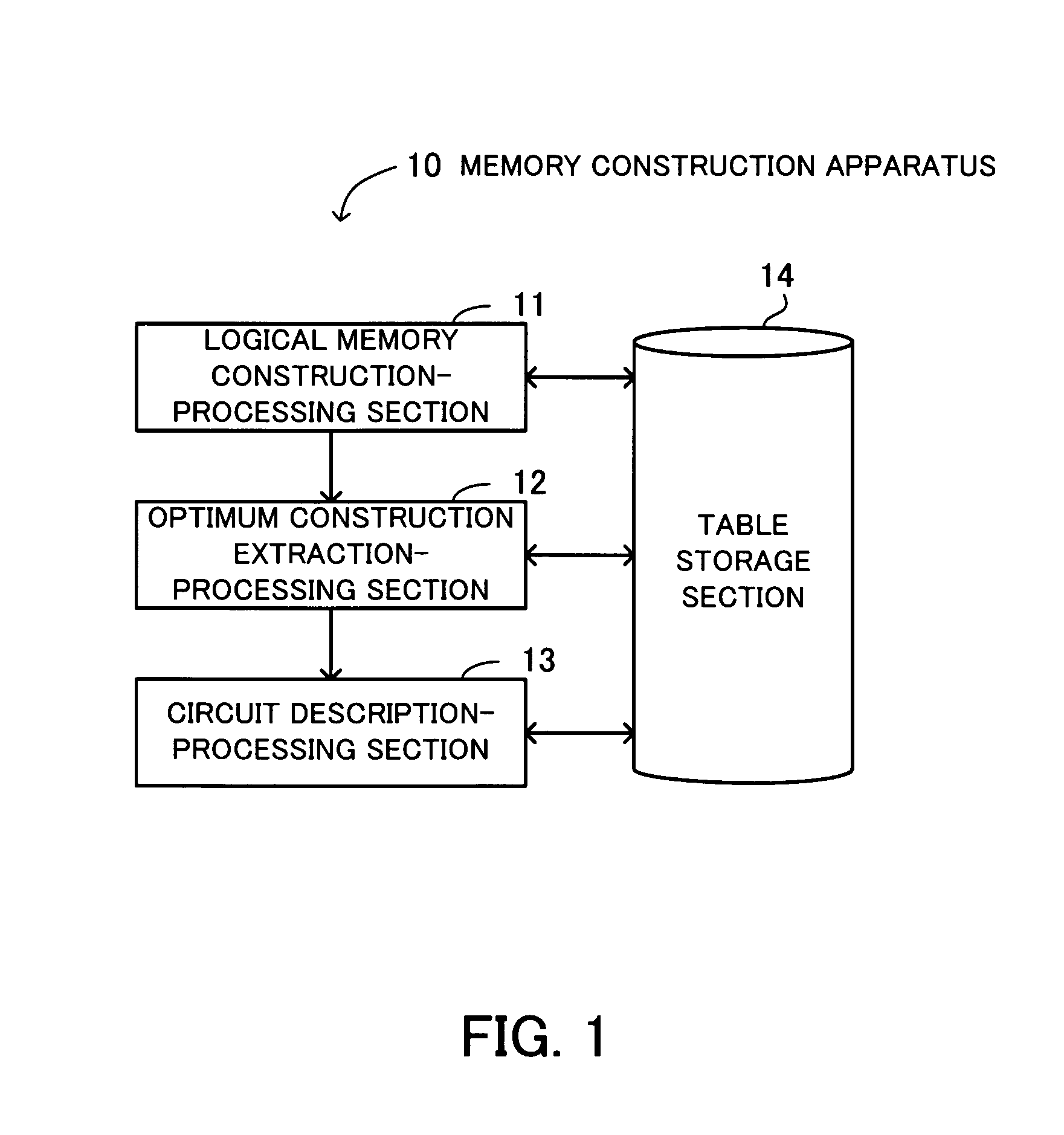
[0047]The invention will now be described in detail with reference to drawings showing a preferred embodiment thereof. FIG. 1 is a diagram useful in explaining the principles of a memory construction apparatus. The memory construction apparatus 10 is hardware in which software for automating and assisting operations for designing electronic equipment, semiconductor devices, and so forth, using EDA (Electronic Design Automation) tools is incorporated, and automatically constructs a logical memory during design of an integrated circuit.

[0048]It should be noted that in the following descriptions, a physical memory is called a physical RAM, and a register an FF (Flip-Flop). Physical RAMs and FFs are memory macros already registered in libraries. Further, the term “logical memory” is intended to mean a memory formed using physical RAMs and FFs, which is constructed by the automatic memory-constructing function of the memory construction apparatus 10 according to the present invention.

[00...


PUM


Abstract

A logical memory construction-processing section reads several kinds of physical memories and registers prepared in advance as libraries, generates candidates for each logical memory, by combining only the physical memories or only the registers, or both the physical memories and the registers, with each other, so as to construct the logical memory that satisfies a logical condition defining a memory space, and selects highest priority candidates for the logical memories from the candidates according to priorities. An optimum construction extraction-processing section extracts optimum logical memories satisfying the respective logical conditions from the highest priority candidates such that the limit numbers of usable physical memories and usable registers are satisfied. A circuit description-processing section executes circuit description by using the physical memories and the registers that construct each of the extracted optimum logical memories, to thereby generate a circuit description file.

Description

CROSS-REFERENCE TO RELATED APPLICATIONS[0001]This application is based upon and claims the benefits of priority from the prior Japanese Patent Application No. 2006-026256 filed on Feb. 2, 2006, the entire contents of which are incorporated herein by reference.BACKGROUND OF THE INVENTION[0002]1. Field of the Invention[0003]This invention relates to a memory construction apparatus, and more particularly to a memory construction apparatus for constructing logical memories in designing an integrated circuit.[0004]2. Description of the Related Art[0005]ASIC (Application Specific Integrated Art) is the generic name for custom ICs (Integrated Circuits) designed e.g. for specific purpose control, and differently from a general-purpose chip, it is a new dedicated chip designed in accordance with specifications desired by an equipment manufacture.[0006]When an equipment manufacturer develops a product, they generally design the product using a general-purpose chip already available, but when ...

Claims


Application Information

Patent Timeline
Patent Type & Authority Patents(United States)
IPC IPC(8): G06F17/50
CPCG06F17/505G06F30/327
Inventor YAMAKAWA, NORITOSHIMIYAMOTO, HIROAKIKOUHARA, YOSHIKATSUNAKAYAMA, AKITSUGUTANDA, KOUICHI
Owner FUJITSU LTD
Why Eureka
Try Eureka