Wireless chip

a wireless chip and chip technology, applied in the near field of read/write/interrogation/identification system, instruments, transmission, etc., can solve the problems of increased size of the ic chip, inability to easily pass magnetic flux due to electromagnetic induction, and malfunction of the circuit included in the ic chip, so as to reduce the size of the wireless chip and the ic chip. , the effect of effective use of a limited area of the chip

Inactive Publication Date: 2010-10-05
SEMICON ENERGY LAB CO LTD
View PDF25 Cites 15 Cited by
  • Summary
  • Abstract
  • Description
  • Claims
  • Application Information

AI Technical Summary

Benefits of technology

[0006]Generally in a wireless chip, an antenna and an IC chip are disposed so as not to overlap each other, since there is fear that an integrated circuit included in the IC chip may malfunction if the antenna and the IC chip are disposed to overlap each other. If the antenna and the IC chip are disposed so as not to overlap each other, however, a large area of the wireless chip is occupied by the antenna and the IC chip. Therefore, magnetic flux due to electromagnetic induction does not pass easily even when, for example, a coil antenna is provided. Further, when capacitors in a storage capacitor portion, a resonance capacitor portion and the like occupy a large area, the size of the IC chip increases, leading to increased size of the wireless chip itself.
[0007]In addition, in the aforementioned case where the wireless chip or the IC chip is large in size, the amount of current required for circuit operation increases. As a result, current consumption increases and the voltage of a power supply may drop, leading to a shorter communication distance and incapability of communication.
[0008]In view of the foregoing, an object of the invention is to provide a wireless chip capable of communicating data wirelessly, the size of which is reduced. A further object of the invention is to reduce the size of an IC chip in the wireless chip, make effective use of a limited area of the chip, reduce current consumption, and prevent communication distance from decreasing.
[0018]According to the invention, an antenna and an IC chip are integrated so as to overlap each other, and the antenna is used as one of two electrodes of a storage capacitor, a resonance capacitor or the like included in the IC chip. Accordingly, the size of a wireless chip and the IC chip can be reduced, leading to effective use of a limited area of the chip, reduction in current consumption, and prevention of decrease in communication distance.

Problems solved by technology

Generally in a wireless chip, an antenna and an IC chip are disposed so as not to overlap each other, since there is fear that an integrated circuit included in the IC chip may malfunction if the antenna and the IC chip are disposed to overlap each other.
Therefore, magnetic flux due to electromagnetic induction does not pass easily even when, for example, a coil antenna is provided.
Further, when capacitors in a storage capacitor portion, a resonance capacitor portion and the like occupy a large area, the size of the IC chip increases, leading to increased size of the wireless chip itself.
In addition, in the aforementioned case where the wireless chip or the IC chip is large in size, the amount of current required for circuit operation increases.
As a result, current consumption increases and the voltage of a power supply may drop, leading to a shorter communication distance and incapability of communication.

Method used


Image

  • Wireless chip
  • Wireless chip
  • Wireless chip

Examples


embodiment mode 1

[0035]In this embodiment mode, a configuration example of a wireless chip according to the invention is described with reference to drawings.

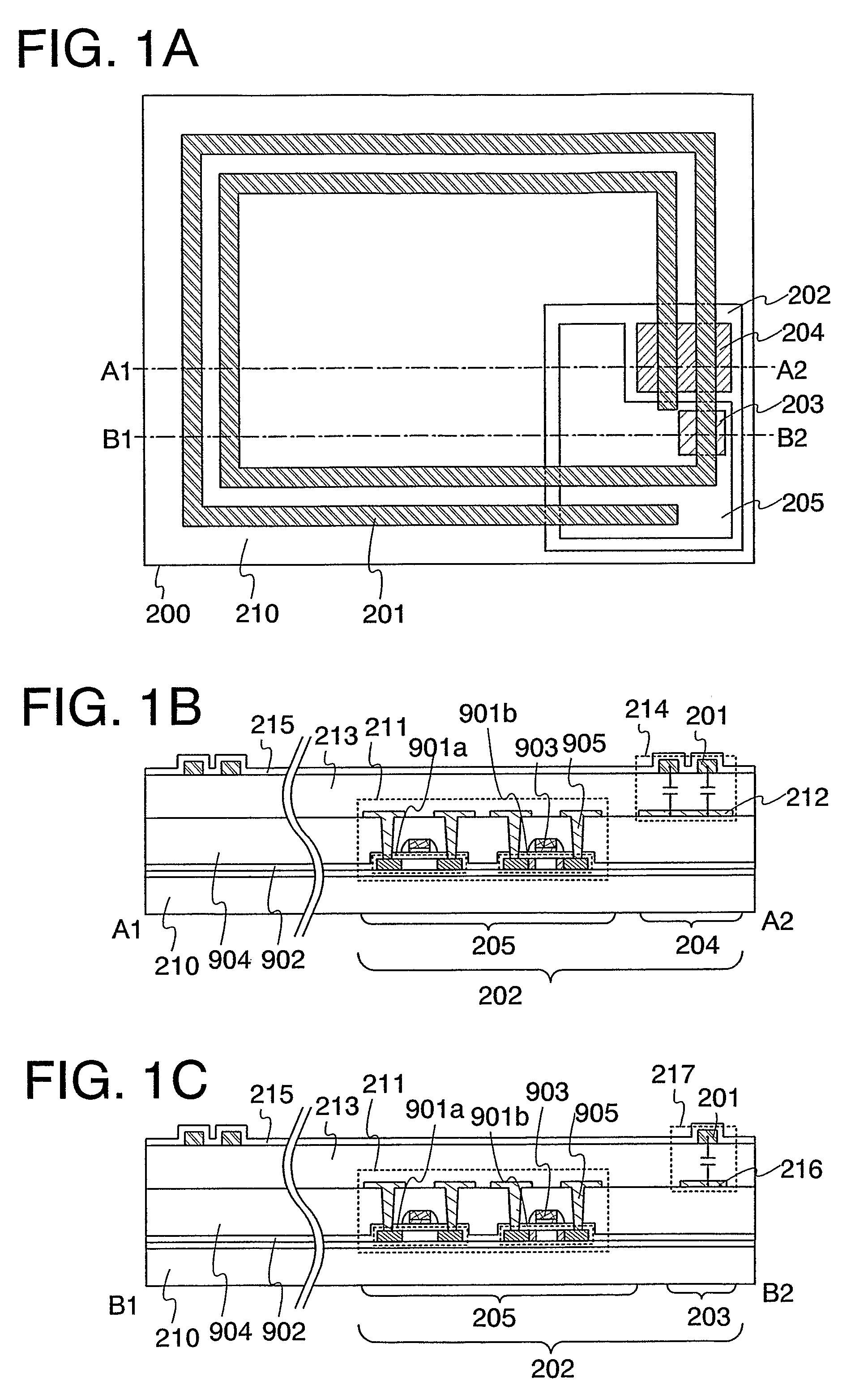
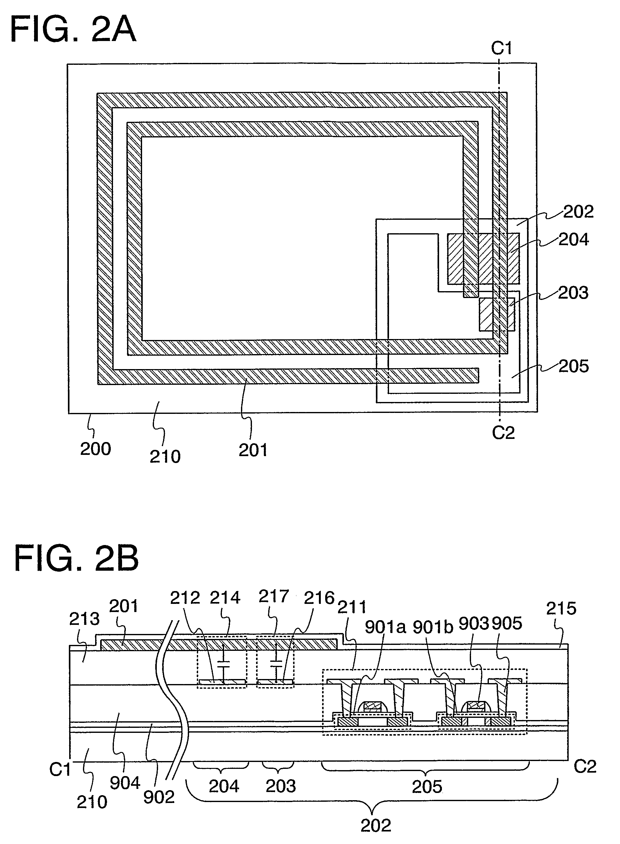
[0036]As shown in FIG. 1A, a wireless chip 200 shown in this embodiment mode includes an antenna 201 and an IC chip 202 that are stacked over the same substrate 210. The antenna 201 and the IC chip 202 are disposed so as to overlap each other at least partially with an insulating film interposed therebetween. The IC chip 202 includes a resonance capacitor portion 204 and a logic portion 205 having a power supply generating means, a control means, a memory means and the like. The logic portion 205 also has a storage capacitor portion 203. Note that the resonance capacitor portion 204 and the storage capacitor portion 203 are selectively disposed in the overlapping area of the antenna 201 and the IC chip 202. The two terminals of the antenna 201 are electrically connected to an integrated circuit of the logic portion 205.

[0037]Each of capacitors ...

embodiment mode 2

[0064]In this embodiment mode, a wireless chip having a different configuration than that of the aforementioned embodiment mode is described with reference to drawings. Specifically, shown is a configuration where an antenna is used as one of two electrodes of a capacitor while a semiconductor film or a gate wiring is used as the other electrode. Note that in this embodiment mode, the same part as the aforementioned embodiment mode is denoted by the same reference numeral.

[0065]FIG. 3B is a cross sectional view of the resonance capacitor portion 204, where the integrated circuit 211 configuring the logic portion 205, the resonance capacitor portion 204 and the antenna 201 are provided over the substrate 210. Note that FIG. 3B corresponds to a cross section taken along a line A1-A2 of the wireless chip 200 shown in FIG. 3A.

[0066]In the resonance capacitor portion 204 shown in FIG. 3B, the antenna 201 and a semiconductor conductive film 252 that is formed using the same material as th...

embodiment mode 3

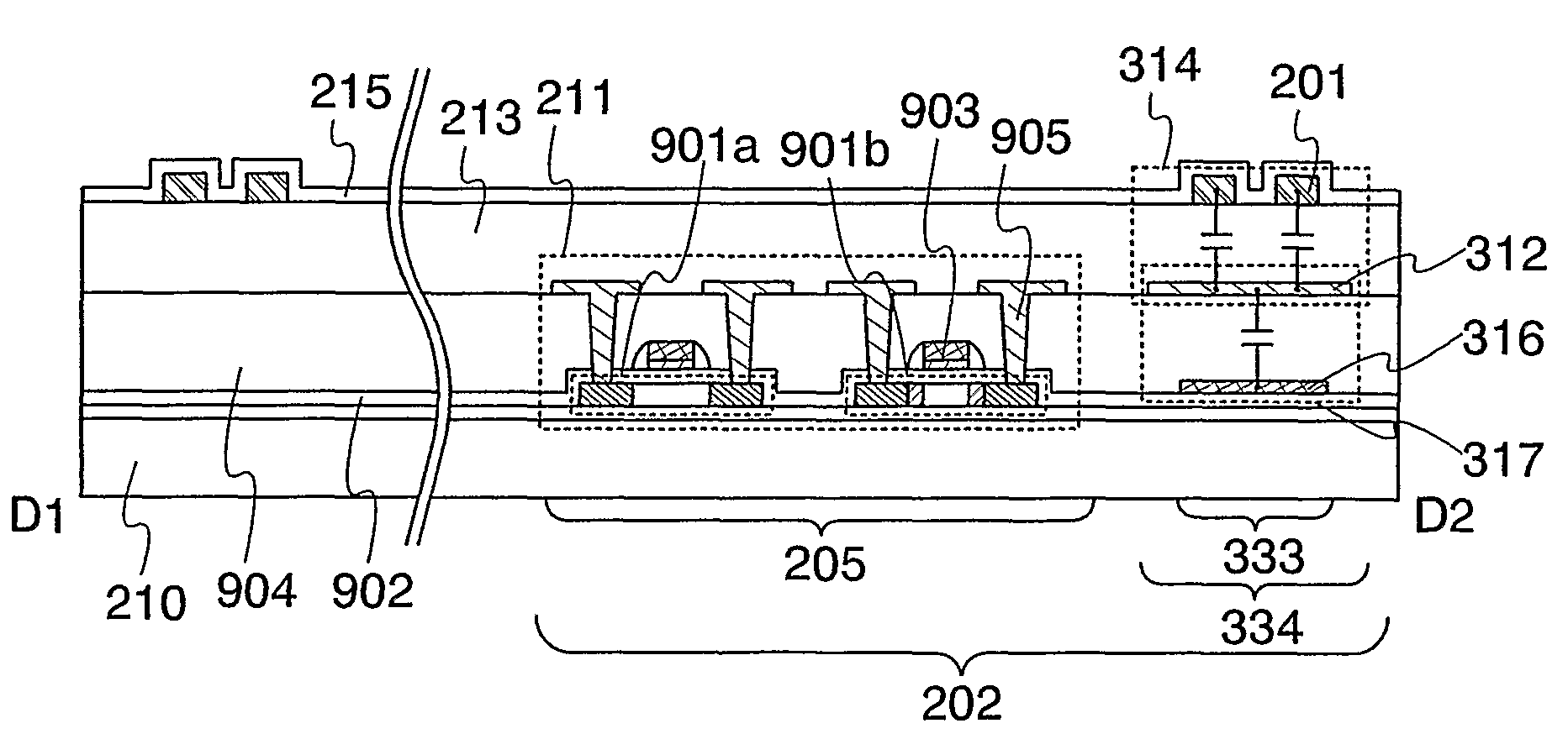
[0076]Described in this embodiment mode is a configuration where the antenna 201 is used as one of two electrodes of a capacitor in a resonance capacitor portion 334 included in the IC chip 202, and the other electrode is used as one of two electrodes of a capacitor in a storage capacitor portion 333, namely, a configuration where the storage capacitor portion and the resonance capacitor portion overlap each other (FIG. 6A).

[0077]FIG. 6B is a cross sectional view of a stacked structure of the storage capacitor portion 333 and the resonance capacitor portion 334, where the integrated circuit 211 configuring the logic portion 205, the storage capacitor portion 333, the resonance capacitor portion 334, and the antenna 201 are provided over the substrate 210. Note that FIG. 6B corresponds to a cross section taken along a line D1-D2 of the wireless chip 200 shown in FIG. 6A.

[0078]In FIG. 6B, a wiring 316 and a wiring 312 are provided with the first interlayer insulating film 904 interpos...


PUM


Abstract

An ID tag capable of communicating data wirelessly, the size of which is reduced, and where the size of an IC chip is reduced, a limited area of the chip is effectively used, current consumption is reduced, and communication distance is prevented from decreasing. The ID tag of the invention includes an IC chip having an integrated circuit, a resonance capacitor portion and a storage capacitor portion, and an antenna formed over the IC chip so as to overlap at least partially with an insulating film interposed therebetween. The antenna, the insulating film and wirings or semiconductor films forming the integrated circuit are stacked, and one or both of capacitors in the resonance capacitor portion and the storage capacitor portion are formed by this stacked structure.

Description

TECHNICAL FIELD[0001]The present invention relates to a wireless chip capable of communicating data wirelessly.BACKGROUND ART[0002]In recent years, with the spread of the Internet, IT (Information Technology) has spread all over the world and revolutionized society. Particularly recently, an environment where the network can be accessed anytime and anywhere has been developed as is called a ubiquitous information society. In such an environment, individual identification systems attract attention, where ID (identification number) is assigned to each object so that the history thereof is revealed and utilized in production, management and the like. Specifically, RFID (Radio Frequency Identification) such as a wireless chip (also called an ID tag, an IC tag, an IC chip, a RF (Radio Frequency) tag, a wireless tag, and an electronic tag) is beginning to be introduced in companies, markets and the like on a trial basis.[0003]In general, a wireless chip 100 is constituted by an antenna 10...

Claims


Application Information

Patent Timeline
Patent Type & Authority Patents(United States)
IPC IPC(8): H01L23/02H01L29/00
CPCG06K19/07749G06K19/0775G06K19/07775G06K19/07779H01L21/84H01L23/5223H01L23/5227H01L27/12H01L27/13H01L29/78612H04B5/0012H01L29/78648H04B5/0056H04B5/0081H01L2924/0002H01L2924/00H01L21/822H01L27/04
Inventor SHIONOIRI, YUTAKA
Owner SEMICON ENERGY LAB CO LTD
Why Eureka
Try Eureka