Flexible oled display with chiplets

a technology of flexible oled and chiplets, which is applied in the direction of discharge tube/lamp details, discharge tube luminescnet screens, organic semiconductor devices, etc., can solve the problems of reducing the conductivity of the electrode, degrading the light-emitting materials, and especially problematic transparent conductive oxides for flexible devices, so as to reduce the bending radius and improve the structure

Active Publication Date: 2010-10-19
GLOBAL OLED TECH
View PDF8 Cites 166 Cited by
  • Summary
  • Abstract
  • Description
  • Claims
  • Application Information

AI Technical Summary

Benefits of technology

[0019]The present invention provides an improved structure for a flexible light-emitting diode device with a reduced bending radius.

Problems solved by technology

However, transparent conductive oxides are especially problematic for flexible devices since they are brittle and subject to cracking when stressed.
The cracking reduces the conductivity of the electrode and can degrade the light-emitting materials.
Thin-film transistors (TFTs) made from amorphous or polycrystalline silicon are relatively large and have lower performance compared to conventional transistors made in crystalline silicon wafers.
Moreover, such thin-film devices typically exhibit local or large-area non-uniformity across the glass substrate that results in non-uniformity in the electrical performance and visual appearance of displays employing such materials.
In flexible applications, the relatively large thin-film components are subject to considerable stress that modifies and degrades the performance of the thin-film components.
However, this thickness is still too large to effectively employ such pixel-control devices on a flexible substrate with a useful bending radius less than 2 cm.
The materials described and tested are not capable of controlling light-emitting elements in a display.

Method used


Image

  • Flexible oled display with chiplets
  • Flexible oled display with chiplets
  • Flexible oled display with chiplets

Examples


Embodiment Construction

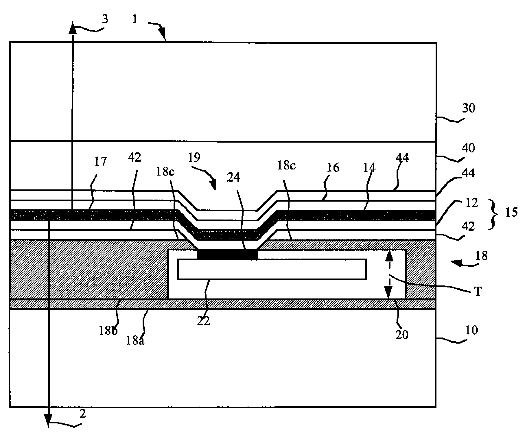
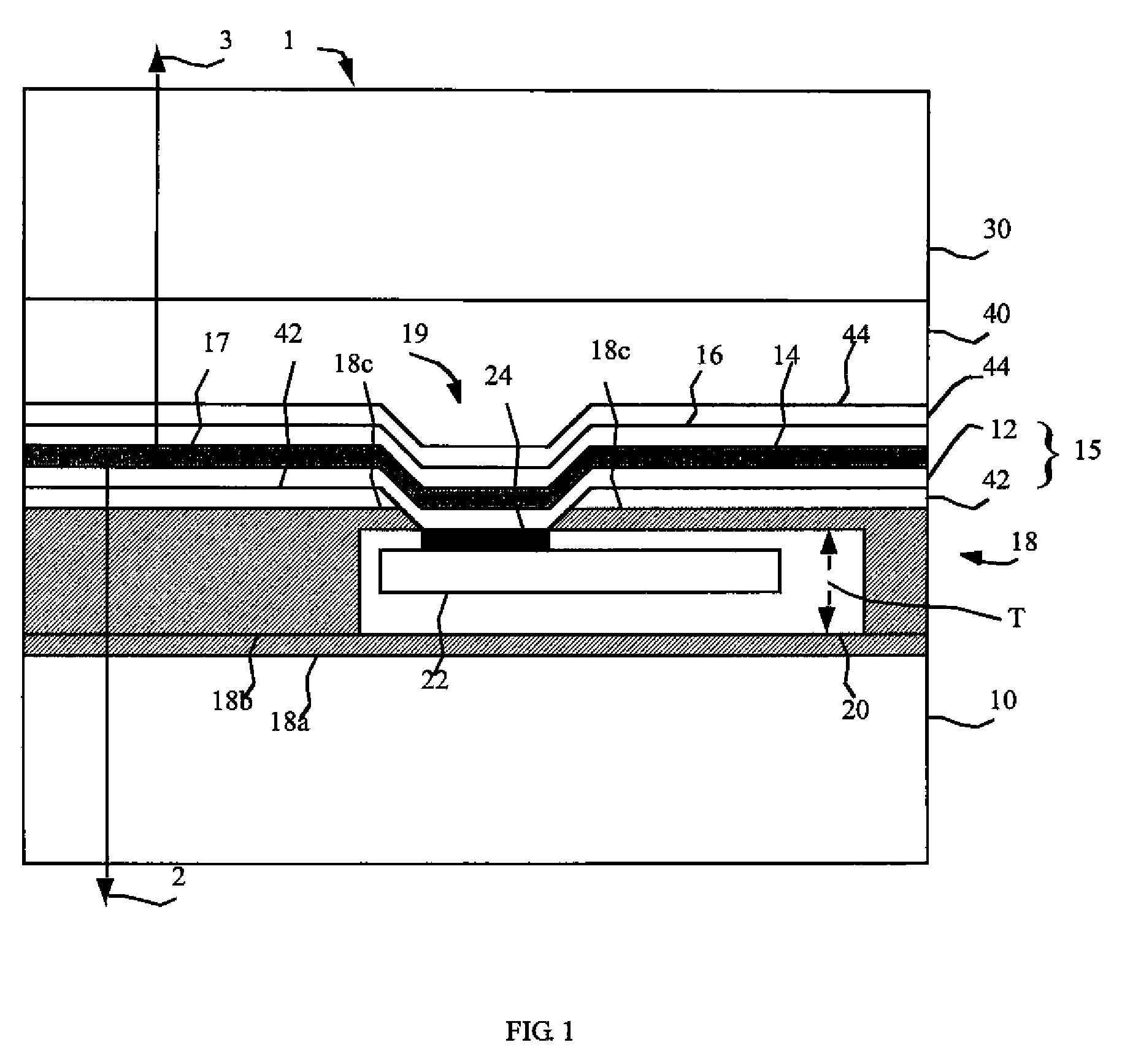
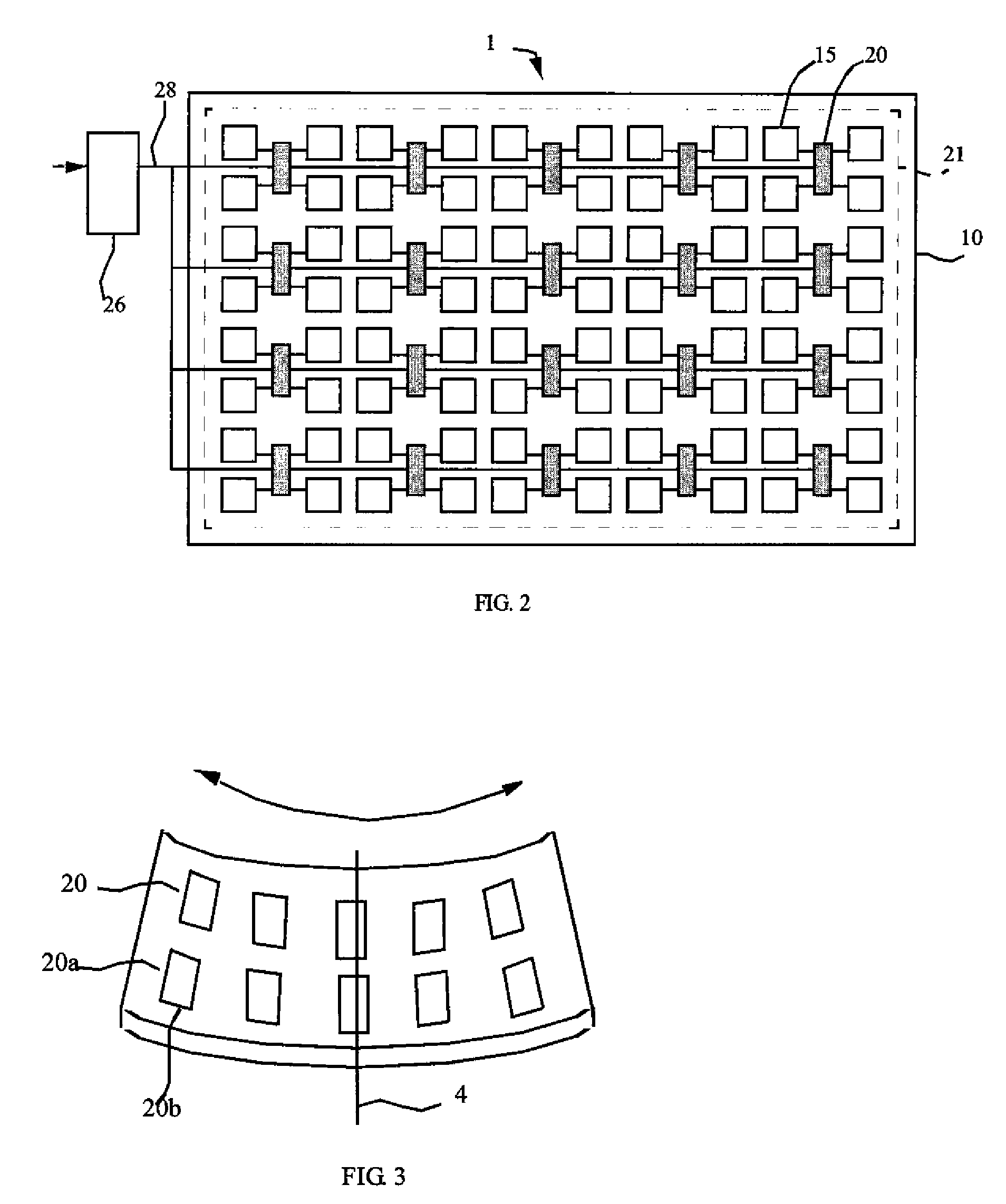
[0023]Referring to FIGS. 1 (in cross section) and 2 (in plan view), in one embodiment of the present invention, a flexible emissive display device 1 comprises a substrate 10 having a display area 21 and an adhesion layer 18 thinner than the substrate 10 formed on the substrate 10 surface. A plurality of chiplets 20 having a thickness T greater than 2 microns and less than 200 microns are adhered to the adhesion layer 18, each chiplet 20 having at least one connection pad 24, the plurality of chiplets 20 distributed within the display area 21, and at least a portion 18c of the adhesion layer 18 extends above the chiplets 20. A plurality of bottom electrodes 12 are formed over the adhesion layer 18 in the display area 21, each bottom electrode 12 is electrically connected to a connection pad 24 of one chiplet 20. At least one layer 14 of light-emitting material is formed over the bottom electrode 12 and a top electrode 16 is formed over the at least one layer 14 of light-emitting mate...


PUM


Abstract

A flexible emissive display device having an adhesion layer thinner than the device substrate; a plurality of chiplets adhered to the adhesion layer wherein at least a portion of the adhesion layer extends above a portion of the chiplets; an OLED formed over the adhesion layer and wherein the OLED is thinner than the adhesion layer; a cover thicker than the adhesion layer located over the OLED and adhered to the device substrate; and wherein the chiplets and OLED are at or near the neutral stress plane of the device and the bending radius of the device is less than 2 cm.

Description

FIELD OF THE INVENTION[0001]The present invention relates to a flexible light-emitting display device employing independent control elements having separate substrates distributed over the device substrateBACKGROUND OF THE INVENTION[0002]Flat-panel display devices are widely used in conjunction with computing devices, in portable devices, and for entertainment devices such as televisions. Such displays typically employ a plurality of pixels distributed over a substrate to display images. Each pixel incorporates several, differently colored, light-emitting elements commonly referred to as sub-pixels, typically emitting red, green, and blue light, to represent each image element. A variety of flat-panel display technologies are known, for example plasma displays, liquid crystal displays, and light-emitting diode displays.[0003]Light emitting diodes (LEDs) incorporating thin films of light-emitting materials forming light-emitting elements have, many advantages in a flat-panel display ...

Claims


Application Information

Patent Timeline
Patent Type & Authority Patents(United States)
IPC IPC(8): H05B33/00
CPCH01L27/3255H01L51/0097H01L27/3262H01L51/5237H01L2251/5338Y02E10/549H10K59/129H10K59/1213H10K77/111H10K2102/311H10K59/8722H10K59/873H10K50/30H10K50/844
Inventor COK, RONALD S.HAMER, JOHN W.
Owner GLOBAL OLED TECH
Why Eureka
Try Eureka