Method for manufacturing resistance RAM device

a technology of resistance ram and ram plate, which is applied in the direction of semiconductor devices, basic electric elements, electrical apparatus, etc., can solve the problems of difficult to achieve a high level of integration, and the ideal etching profile is not obtained in the etching process for forming patterns, so as to achieve secure switching characteristics and reduce the size of the reram

Active Publication Date: 2010-11-16
SK HYNIX INC
View PDF6 Cites 23 Cited by
  • Summary
  • Abstract
  • Description
  • Claims
  • Application Information

AI Technical Summary

Benefits of technology

[0011]An embodiment of the present invention is directed to a method for manufacturing an ReRAM device which can secure switching characteristics in spite of the decrease in the size of an ReRAM.

Problems solved by technology

In order to obtain a high charge storing capacity, the surface area of an electrode must be increased, thereby making it difficult to accomplish a high level of integration.
This also in turn makes it difficult to accomplish a high level of integration.
However in conventional ReRAM devices, an ideal etching profile is not obtained in an etching process for forming patterns, and the sides of the top electrode tend to be etched to a great extent.
This in turn causes a problem in that the switching characteristics of the ReRAM device are likely to deteriorate.
In particular, when the size of an ReRAM device is decreased, the areas of the TMO and the top electrode are decreased in comparison to the area of the bottom electrode; and therefore the conventional ReRAM device has a drawback in that switching characteristics cannot be secured.

Method used


Image

  • Method for manufacturing resistance RAM device
  • Method for manufacturing resistance RAM device
  • Method for manufacturing resistance RAM device

Examples


Embodiment Construction

[0022]Hereafter, a specific embodiment of the present invention will be described in detail with reference to the accompanying drawings.

[0023]FIGS. 1A through 1E are cross-sectional views shown for illustrating the processes of a method for manufacturing a resistance RAM device in accordance with an embodiment of the present invention. The method will be described below.

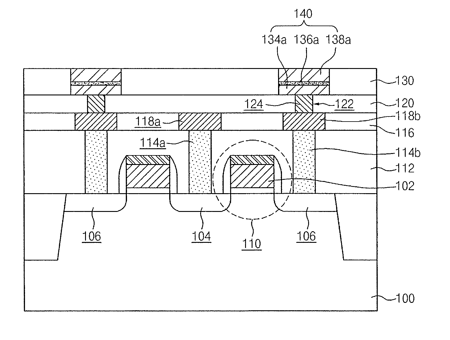
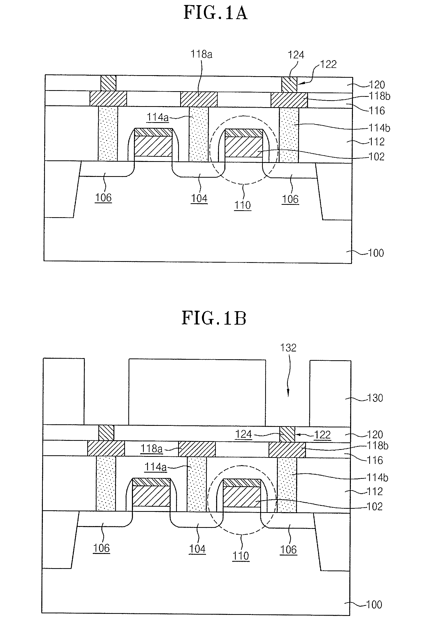
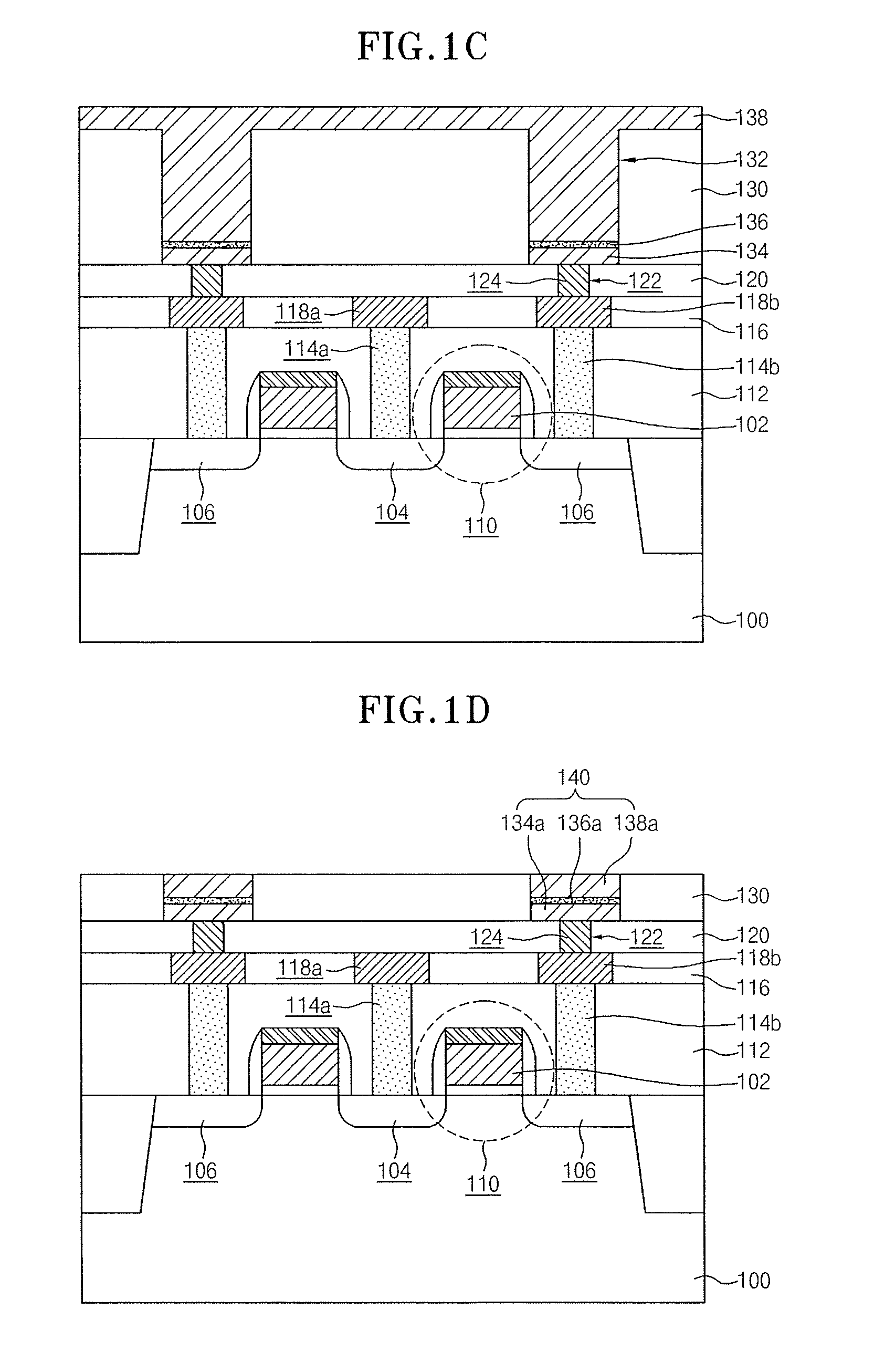
[0024]Referring to FIG. 1A, a switching element 110, which comprises a transistor including a gate 102, a source region 104 and a drain region 106, is formed on a semiconductor substrate 100. After forming a first interlayer dielectric 112 on the semiconductor substrate 100 to cover the switching element 110, first and second contact plugs 114a and 114b, which are electrically connected to the source region 104 and the drain region 106, respectively, are formed in the first interlayer dielectric 112 according to a process well known in the art.

[0025]After forming a first insulation layer 116 on the first interlayer d...


PUM


Abstract

Manufacturing a resistance RAM device includes the steps of forming an insulation layer on a semiconductor substrate having a bottom electrode contact; etching the insulation layer to define a hole exposing the bottom electrode contact; depositing sequentially a bottom electrode material layer and a TMO material layer selectively within the hole; depositing a top electrode material layer within the hole and on the insulation layer in such a way as to completely fill the hole in which the bottom electrode material layer and the TMO material layer are formed; removing partial thicknesses of the top electrode material layer and the insulation layer to form a stack pattern comprising a bottom electrode, a TMO, and a top electrode.

Description

CROSS-REFERENCE TO RELATED APPLICATIONS[0001]The present application claims priority to Korean patent application number 10-2008-0137336 filed on Dec. 30, 2008, which is incorporated herein by reference in its entirety.BACKGROUND OF THE INVENTION[0002]The present invention relates generally to a method for manufacturing a resistance RAM device, and more particularly, to a method for manufacturing a resistance RAM device, which can secure switching characteristics.[0003]Memory devices can generally be classified as volatile random access memory (RAM), which requires power to maintain stored information, or nonvolatile read only memory (ROM), which can retain the stored state of inputted information even when power is interrupted. Examples of volatile RAM include dynamic RAM (DRAM) and an static (SRAM), and an example of nonvolatile ROM is a flash memory device such as electrically erasable and programmable ROM (EEPROM).[0004]Typical DRAM devices are generally considered excellent mem...

Claims


Application Information

Patent Timeline
Patent Type & Authority Patents(United States)
IPC IPC(8): H01L21/4763
CPCH01L45/04H01L45/1233H01L45/146H01L45/147H01L45/1625H01L45/1666H01L27/2436H10B63/30H10N70/20H10N70/826H10N70/8833H10N70/8836H10N70/026H10N70/061H10N50/01H10B99/00
Inventor LEE, YU JIN
Owner SK HYNIX INC
Why Eureka
Try Eureka