
Substrate carrying and processing apparatus

a technology for carrying and processing substrates, applied in lighting and heating apparatus, charge manipulation, furnaces, etc., can solve the problems of complex carrying schedules and risk of occurrence of defects, and achieve the effects of enhancing throughput, substantial downsizing of the apparatus, and increasing the number of substrates

Active Publication Date: 2010-11-23
TOKYO ELECTRON LTD
View PDF12 Cites 21 Cited by
  • Summary
  • Abstract
  • Description
  • Claims
  • Application Information

AI Technical Summary

Benefits of technology

[0012]The present invention was made in light of the above circumstances, and it is therefore an object of this invention to provide a substrate carrying and processing apparatus which can achieve substantial downsizing of the apparatus, increase the number of substrates to be stored therein, and enhance the throughput.

Problems solved by technology

If the substrate is not cooled immediately after the heating process, there is a risk of occurrence of defects due to overheating or over-baking of the substrate.
Therefore, the carrying schedule for respective substrates should be more complicated.

Method used


Image

  • Substrate carrying and processing apparatus
  • Substrate carrying and processing apparatus
  • Substrate carrying and processing apparatus

Examples


examples

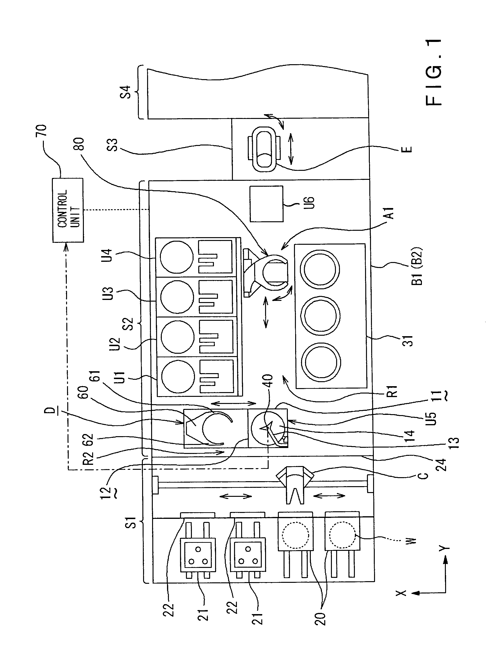
[0045]Hereinafter, one example which is considered to be the most preferred embodiment of the present invention will be described with reference to the attached drawings. In the description, a case where a substrate carrying and processing apparatus according to the present invention is applied to a resist coating and developing apparatus utilized for semiconductor wafers is discussed.

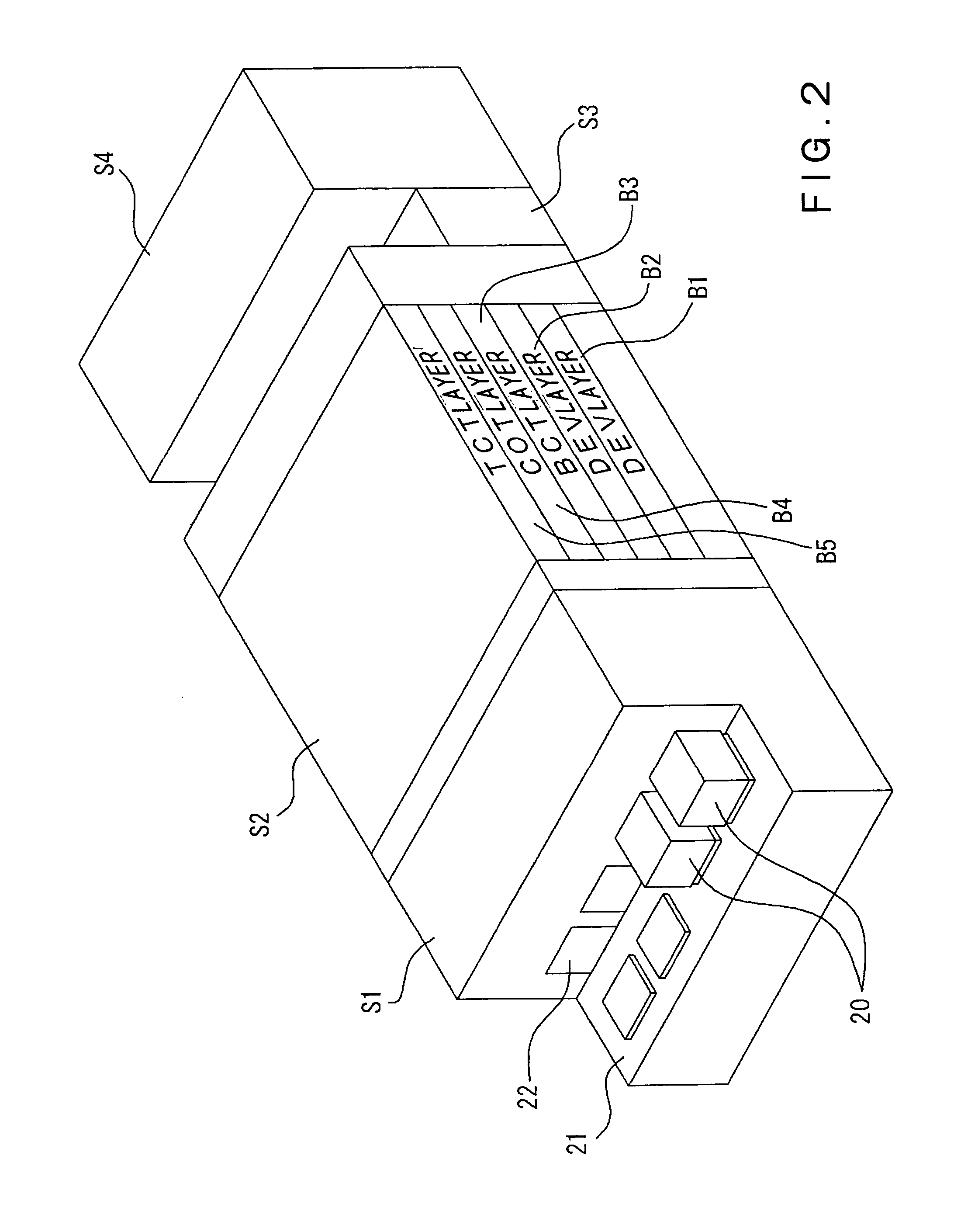
[0046]FIG. 1 is a schematic plan view showing one example of the resist coating and developing apparatus, FIG. 2 is a schematic perspective view of the same apparatus, and FIG. 3 is a schematic view of the same apparatus, illustrating a general configuration of unit blocks of a processing section, the unit blocks being expressed in a plan view and in a stacked state.

[0047]The resist coating and developing apparatus comprises a carrier block S1 which is configured to carry in and carry out carriers 20 each receiving thirteen sheets, for example, of semiconductor wafers W (hereinafter, referred to as waf...


PUM

PropertyMeasurementUnit
angleaaaaaaaaaa
thicknessaaaaaaaaaa
temperatureaaaaaaaaaa

Abstract

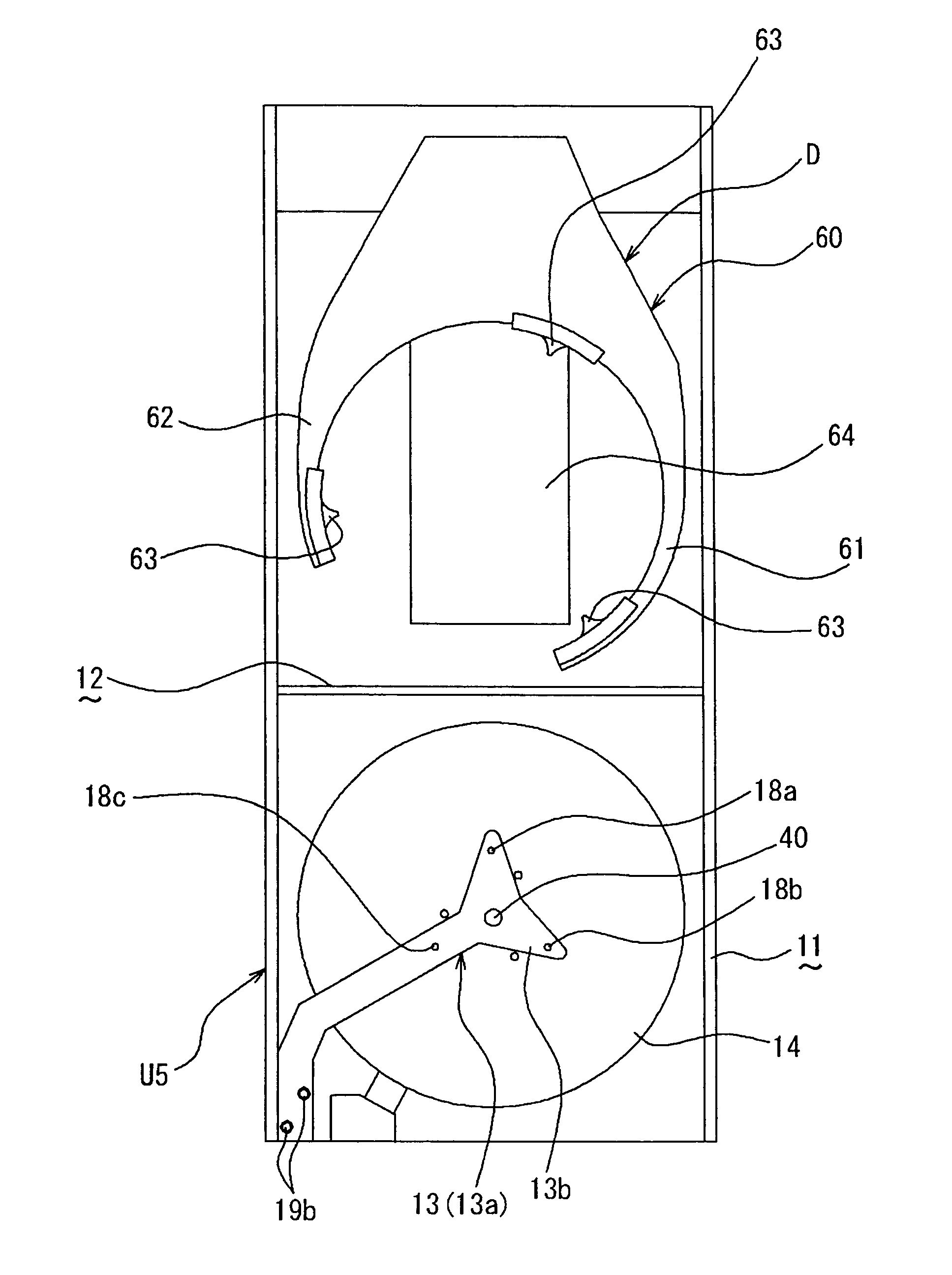
The present invention provides a substrate carrying and processing apparatus which is intended to reduce the size of the space for storing substrates in each substrate storing section as much as possible so as to downsize the apparatus and increase the number of substrates to be stored therein as well as to enhance the throughput. The substrate carrying and processing apparatus comprises a carrier block S1 which is adapted to position carriers 20 each receiving wafers W therein, a processing block S2 including processing units U1 to U4, 31 used for processing each wafer, a main arms A1 adapted to transfer each wafer to each processing unit, a rack unit U5 which is disposed between the carrier block and the processing block and able to store wafers to be processed, and a transfer arm D adapted to transfer each wafer to the rack unit. The rack unit has openings 11, 12 to which the main arm and the transfer arm can transfer each substrate along two directions crossing to each other, and includes a plurality of placing shelves with a space therebetween and adapted to support a wafer. The main arms and transfer arms are configured such that they can be advanced into and retracted from the substrate storing section and such that they can be overlapped to the corresponding placing shelf in the vertical direction, when viewed in the horizontal direction.

Description

BACKGROUND OF THE INVENTION[0001]1. Field of the Invention[0002]The present invention relates to a substrate carrying and processing apparatus which is adapted to carry and process a substrate, for example, a semiconductor wafer or LCD glass substrate.[0003]2. Background Art[0004]Generally, in production of semiconductor devices, a photolithography technique is utilized to form a thin film of ITO (Indium Tin Oxide) and / or electrode pattern on a substrate, such as a semiconductor wafer or LCD glass substrate. The photolithography technique is performed in a series of steps comprising; coating a photoresist on a substrate, exposing the resultant resist film which corresponds to a predetermined circuit pattern, and then developing the exposed pattern so as to form a desired circuit pattern of the resist film.[0005]An apparatus for performing such processes is generally provided with a resist coating and processing unit adapted to coat and process a resist liquid on a substrate, a heati...

Claims


Application Information

Patent Timeline
Patent Type & Authority Patents(United States)
IPC IPC(8): B05C13/02B05C11/00B05B15/12B65G49/07
CPCH01L21/67742H01L21/67748H01L21/67769H01L21/68707Y10S414/141Y10S414/136Y10S414/14H01L21/68
Inventor TANOUE, MITSUHIROENOKIDA, SUGURU
Owner TOKYO ELECTRON LTD
Learn More