Circuit board structure having embedded semiconductor element and fabrication method thereof

a semiconductor element and circuit board technology, applied in the direction of printed circuit manufacturing, printed circuit non-printed electric components association, electrical apparatus construction details, etc., can solve the problems of warpage or deformation, different degrees of deformation or shrinkage, and the semiconductor element embedded in the core circuit board is susceptible to damage, so as to improve the reliability and quality of the circuit board structure, prevent warpage or delamination, and enhance the rigidity of the carrier board

Active Publication Date: 2010-11-23
UNIMICRON TECH CORP
View PDF9 Cites 40 Cited by
  • Summary
  • Abstract
  • Description
  • Claims
  • Application Information

AI Technical Summary

Benefits of technology

[0017]In view of the disadvantages of the prior art mentioned above, it is a primary objective of the present invention to provide a circuit board structure that has an embedded semiconductor element and a fabrication method thereof, which are capable of increasing the rigidity of the circuit board structure and thereby preventing warpage.
[0018]It is another objective of the present invention to provide a circuit board structure that has an embedded semiconductor element and its fabrication method, which are capable of enhancing reliability of the circuit board structure.
[0019]It is a further objective of the present invention to provide a circuit board structure that has an embedded semiconductor element and a fabrication method thereof, which are capable of mounting at least one semiconductor element, e.g. active or inactive element, inside substrate, thus to enhance electrical capability of the circuit board structure.

Problems solved by technology

However, based on practical demand of circuit design, the purposes of the upper and the lower surfaces of the core circuit board are different; therefore, the circuit layout of the upper surface of the core circuit board is frequently different from the circuit layout of the lower surface of the core circuit board, besides, the differences between the coefficient of thermal expansion of the metallic conductive layers and insulating layers and solder masks are great, when temperature changes in the fabrication process, situations of warpages happen frequently; in addition, when circuit density of one surface of the core circuit board is higher than the circuit density of the other surface, temperature changes that happen in processes of, e.g. baking, encapsulant curing, and thermal cycle, will generate different thermal stresses on the upper and the lower surfaces of the core circuit board, therefore, the two surfaces of the core circuit board will generate different degrees of deformation or shrinkage, in other words, warpage will happen to the core circuit board, in a more serious situation, delamination occurs between layers of the circuit board.
To meet the demand for high integration, sides of the circuit board for mounting semiconductor elements on must be fabricated to have matching multiple circuit layers of high density and fine circuit, oppositely, sides on the circuit board for mounting external electronic devices on does not have the same matching high wiring density as the sides for mounting chips, thus warpage is prone to happen, and also the semiconductor element embedded in the core circuit board is susceptible to damage due to uneven thermal stress.
A difference in the coefficients of thermal expansion between different components of a semiconductor package generates thermal stress that, in turn, causes uneven thermal stress to the surfaces of the package structure, therefore, situations of warpage or delamination are prone to happen in the fabrication process and then indirectly affect reliability and quality of products.
Besides, the number of circuit layers of the circuit build-up structure is limited by warpage; in other words, warpage renders a high level and a great number of circuit layers integration impossible and further prevents the development of semiconductor devices from high integration and miniaturization.
Hence, it is a highly urgent issue in the circuit board industry as to how to provide a circuit board structure that has an embedded semiconductor element, in order to overcome the aforementioned drawback regarding poor anti-flexural strength of a circuit board structure as found in the prior art.

Method used


Image

  • Circuit board structure having embedded semiconductor element and fabrication method thereof
  • Circuit board structure having embedded semiconductor element and fabrication method thereof
  • Circuit board structure having embedded semiconductor element and fabrication method thereof

Examples


first embodiment

[0041]Please refer to FIGS. 2A through 2E, which are cross-sectional views of the first embodiment of a circuit board structure having an embedded semiconductor element and a fabrication method thereof according to the present invention.

[0042]As shown in FIG. 2A, first, providing a carrier board 21 that is either an insulating board or a ceramic plate, wherein the carrier board 21 has a first surface 21a, a second surface 21b, and at least one through hole 210 penetrating the carrier board from the first surface 21a to the second surface 21b; mounting at least one second semiconductor element 22 on the second surface 21b of the carrier board 21, wherein the second semiconductor element 22 has an active surface 22a and an inactive surface 22b and is mounted on the second surface 21b of the carrier board 21 via the inactive surface 22b, and the active surface 22a of the second semiconductor element 22 has a plurality of electrode pads 221; the second semiconductor element is either an...

second embodiment

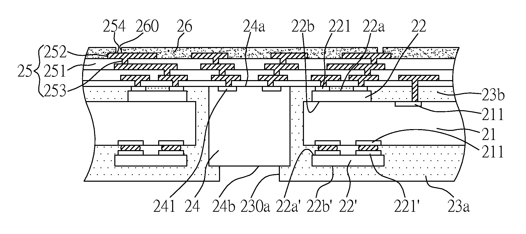
[0050]Please refer to FIGS. 3A through 3E, which are cross-sectional views of the second embodiment of a circuit board structure having an embedded semiconductor element and a fabrication method thereof according to the present invention, the main difference from the first embodiment is that the carrier board of the second embodiment is a circuit board.

[0051]As shown in FIG. 3A, first provide a carrier board 21 that is a circuit board, the circuit board has a single-layered circuit or a multi-layered circuit, and the circuit board 21 has a first surface 21a, a second surface 21b, and at least one through hole 210 penetrating the carrier board from the first surface 21a to the second surface 21b; form a plurality of electrically connecting pads 211 on both the first surface 21a and the second surface 21b; next, mount a plurality of second semiconductor elements 22 and 22′ on the second surface 21b and the first surface 21a of the carrier board 21 respectively, the second semiconducto...


PUM


Abstract

A circuit board structure with an embedded semiconductor element and a fabrication method thereof are disclosed according to the present invention. The circuit board structure comprises: a carrier board having a first surface, a second surface, and at least one through hole penetrating the carrier board from the first surface to the second surface; a first semiconductor element received in the through hole and having an active surface and an inactive surface, the active surface having a plurality of electrode pads; at least one second semiconductor element mounted on the carrier board; a first encapsulation layer formed on the first surface of the carrier board to block one end of the through hole; and a second encapsulation layer formed on the second surface of the carrier board.

Description

CROSS-REFERENCE TO RELATED APPLICATIONS[0001]Under 35 U.S.C. §119(e), this application claims the benefit of priority to Taiwanese Patent Application No. 095148700, filed Dec. 25, 2006. All of which is incorporated herein by reference.BACKGROUND OF THE INVENTION[0002]1. Field of the Invention[0003]This invention generally relates to a circuit board structure and a fabrication method thereof, and more specifically, to a circuit board structure with an embedded semiconductor element and a fabrication method thereof.[0004]2. Description of Related Art[0005]As the electronic industry vigorously flourishes, designs of electronic products are trending toward low weight, small thickness, and small size, and the developing trend of product functions has been gradually towards high performance, high capability, and high speed. In order to meet the demand for high integration and miniaturization of semiconductor devices, the circuit board that provides a plurality of active / inactive elements ...

Claims


Application Information

Patent Timeline
Patent Type & Authority Patents(United States)
IPC IPC(8): H05K1/18
CPCH01L23/5389H01L24/24H01L24/82H01L24/19H01L2224/24227H01L2224/82039H01L2924/01009H01L2924/14H01L2924/18162H01L2924/19041H01L2924/19042H01L2924/19043H05K1/185H05K3/4602H01L2924/01006H01L2924/01033H01L2924/014H01L2924/351H01L2224/04105H01L2224/16227H01L2224/73267H01L2924/00
Inventor HSU, SHIH-PING
Owner UNIMICRON TECH CORP
Why Eureka
Try Eureka