Processing a printed wiring board by single bath electrodeposition

Inactive Publication Date: 2010-12-07
LAWRENCE LIVERMORE NAT SECURITY LLC
View PDF12 Cites 8 Cited by
  • Summary
  • Abstract
  • Description
  • Claims
  • Application Information

AI Technical Summary

Benefits of technology

[0011]In an embodiment of the present invention plating of copper on the printed wiring board from a bath containing nickel and copper is conducted using a low reduction potential and is conducted with high agi

Problems solved by technology

By not flowing detrimentally, it is meant that any flow of the thin layer of tin-lead solder will be insufficient to cause bridging or wrinkling and/or rupture of a solder mask on top of it.
Additionally, such

Method used


Image

  • Processing a printed wiring board by single bath electrodeposition
  • Processing a printed wiring board by single bath electrodeposition
  • Processing a printed wiring board by single bath electrodeposition

Examples


Embodiment Construction

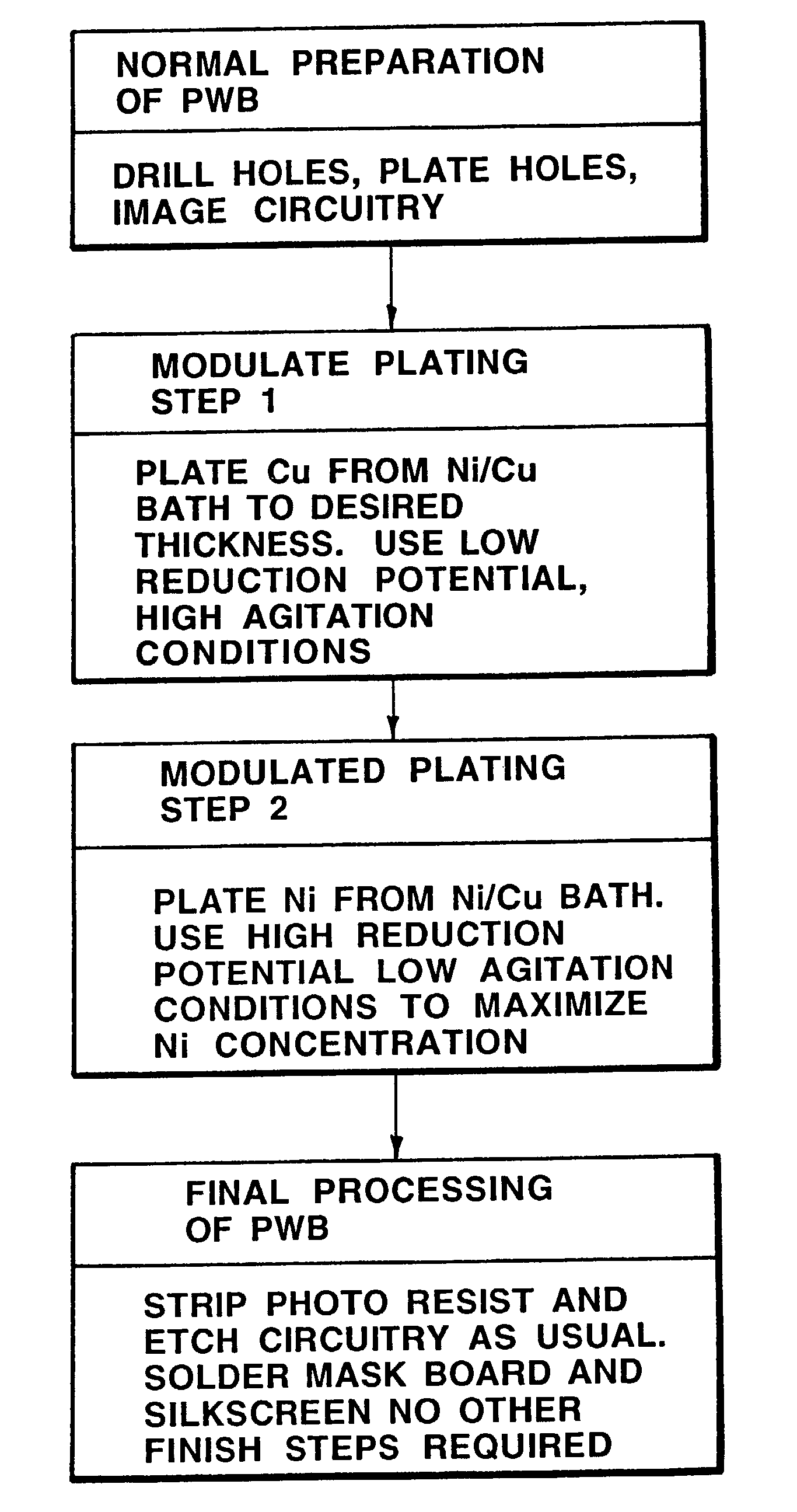
[0017]Referring now to the drawings, specific embodiments of the invention are shown. The detailed description of the specific embodiments, together with the general description of the invention, serve to explain the principles of the invention.

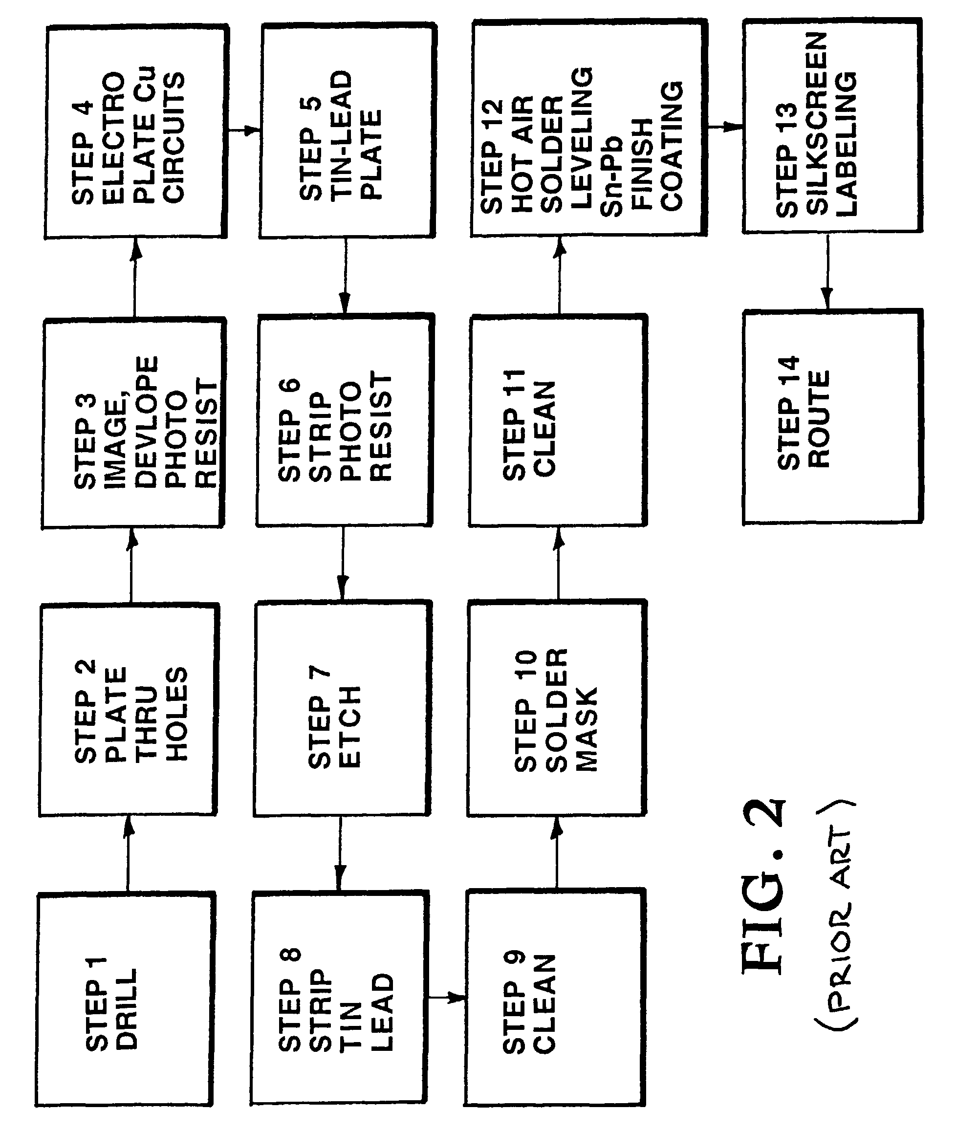
[0018]Hot-air solder leveling (HASL), the most common method of finishing printed wiring boards (PWBs), is one of the main uses of lead in traditional PWB manufacturing. Unfortunately, the HASL technology includes some environmental and human health risks. One of the major risks associated with printed wiring board (PWB) manufacture is the use of lead. Replacing or simplifying HASL will lead to both employee health and environmental benefits. In addition, there is a production advantage to eliminating or simplifying HASL, for it provides a fairly uneven surface that is problematic for mounting very small components.

[0019]The printed wiring board industry has low profit margins on many of its products. In the PWB process the “footprint,” the t...


PUM

PropertyMeasurementUnit
Lengthaaaaaaaaaa
Lengthaaaaaaaaaa

Abstract

A method of processing a printed wiring board. Initial processing steps are implemented on the printed wiring board. Copper is plated on the printed wiring board from a bath containing nickel and copper. Nickel is plated on the printed wiring board from a bath containing nickel and copper and final processing steps are implemented on the printed wiring board.

Description

CROSS-REFERENCE TO RELATED APPLICATIONS[0001]This application is a division of application Ser. No. 09 / 810,877 filed Mar. 16, 2001 now U.S. Pat. No. 6,547,946. This application claims the benefit of U.S. Provisional Application No. 60 / 195,479, filed Apr. 10, 2000, entitled “Use of Layered Plating Techniques in Printed Circuit Board Manufacture,” which is incorporated herein by this reference.[0002]The United States Government has rights in this invention pursuant to Contract No. W-7405-ENG-48 between the United States Department of Energy and the University of California for the operation of Lawrence Livermore National Laboratory.BACKGROUND OF THE INVENTION[0003]1. Field of Endeavor[0004]The present invention relates to printed wiring boards and more particularly to a single bath electrodeposition system.[0005]2. State of Technology[0006]U.S. Pat. No. 3,770,571 for fabrication of printed circuit boards by Henry Alsberg and Ronald A. Frederiksen, patented Nov. 6, 1973, provides the f...

Claims


Application Information

Patent Timeline
IPC IPC(8): C25D5/10B32B3/00C25D3/56C25D3/58C25D5/12H05K3/06H05K3/24
CPCC25D3/562C25D3/58H05K3/244C25D5/12Y10T428/24917H05K3/062C25D5/627C25D5/611
Inventor MELTZER, MICHAEL P.STEFFANI, CHRISTOPHER P.GONFIOTTI, RAY A.
Owner LAWRENCE LIVERMORE NAT SECURITY LLC
Why Eureka
Try Eureka