Treatment method for surface of substrate, method of fabricating image sensor by using the treatment method, and image sensor fabricated by the same

a technology of substrate surface and treatment method, which is applied in the direction of electrical equipment, radio frequency control devices, semiconductor devices, etc., can solve the problems of light entering the micro-lens at an angle that may not reach the density of the cmos image sensor may be increased, and the limitation of the active pixel sensor array region. , to achieve the effect of reducing the quantity of light entering the photoelectric transformation unit, and reducing the quantity of ligh

Inactive Publication Date: 2010-12-21
SAMSUNG ELECTRONICS CO LTD
View PDF4 Cites 6 Cited by
  • Summary
  • Abstract
  • Description
  • Claims
  • Application Information

AI Technical Summary

Benefits of technology

[0007]Example embodiments provide a substrate surface treatment method to remove defects created on the surface of the substrate. Example embodiments provide a method of fabricating an image sensor that may improve low illumination characteristics using the substrate surface treatment method above. Example embodiments provide an image sensor fabricated using the methods above.
[0012]Although a micro-lens that gathers light is used in an image sensor, light entering the micro-lens at an angle may not reach a photoelectric transformation unit. As a result, the quantity of light may be reduced and the photosensitivity of the image sensor may be lowered. Also, the quantity of light that arrives at the photoelectric transformation unit may be reduced due to the distance between the micro-lens and the photoelectric transformation unit, which decreases the photosensitivity of the image sensor.
[0013]Methods to prevent or reduce deterioration of photosensitivity of an image sensor may include a method that shortens the path of light entering a phototransformation unit by allowing light to enter from the back side of a semiconductor substrate. However, the method allowing light to enter from the back side of the semiconductor substrate may suffer disadvantages, e.g., low illumination, when the back side of the semiconductor substrate may be contaminated or may contain surface defects. When light enters the back side of the semiconductor substrate, electric charges or hole carriers may be created on the back side surface of the semiconductor substrate. As a result, the low illumination characteristic, e.g., a leak current, may increase on the back side of the semiconductor substrate, may deteriorate.

Problems solved by technology

Although the integration density of a CMOS image sensor may be increased, increasing the size of the active pixel sensor array region has shown limitations.
Although a micro-lens that gathers light is used in an image sensor, light entering the micro-lens at an angle may not reach a photoelectric transformation unit.
However, the method allowing light to enter from the back side of the semiconductor substrate may suffer disadvantages, e.g., low illumination, when the back side of the semiconductor substrate may be contaminated or may contain surface defects.
As a result, the low illumination characteristic, e.g., a leak current, may increase on the back side of the semiconductor substrate, may deteriorate.

Method used


Image

  • Treatment method for surface of substrate, method of fabricating image sensor by using the treatment method, and image sensor fabricated by the same
  • Treatment method for surface of substrate, method of fabricating image sensor by using the treatment method, and image sensor fabricated by the same
  • Treatment method for surface of substrate, method of fabricating image sensor by using the treatment method, and image sensor fabricated by the same

Examples


Embodiment Construction

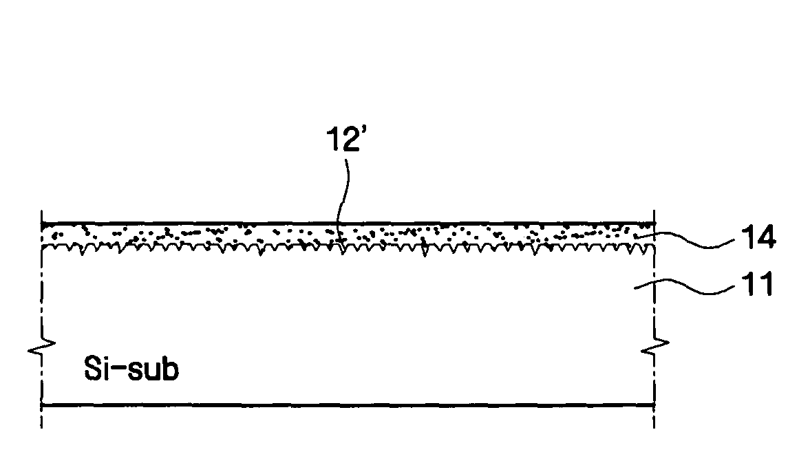
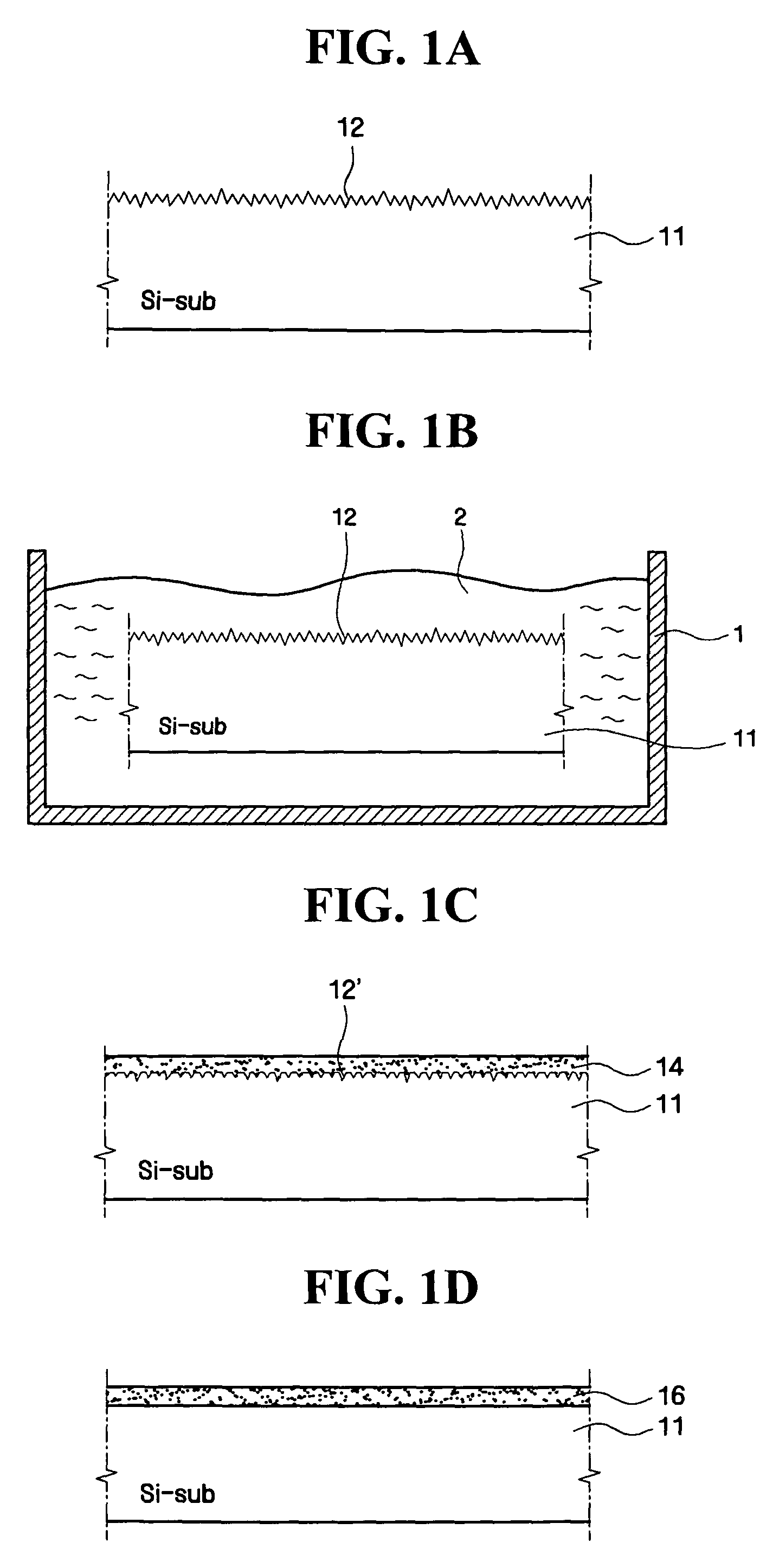
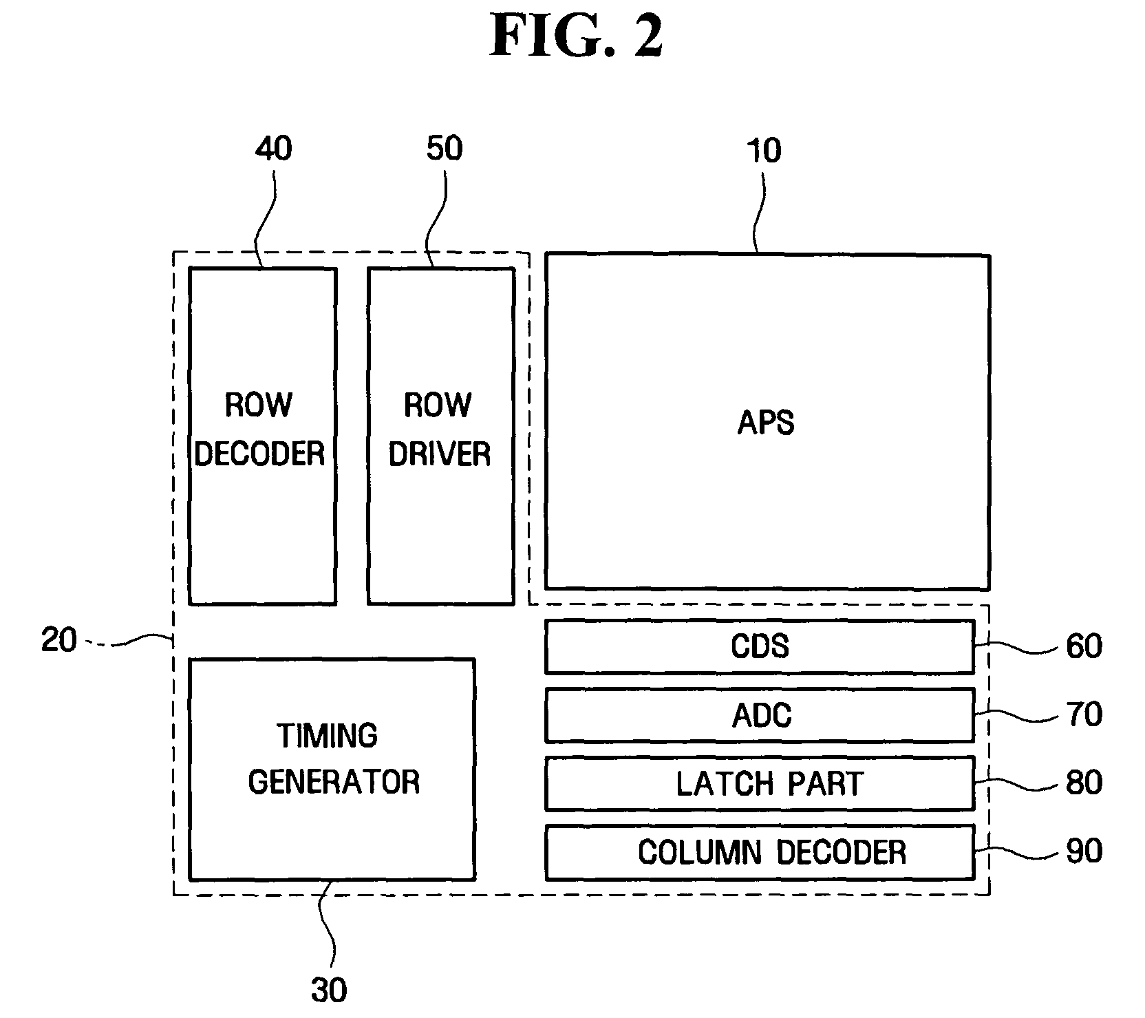
[0025]Advantages and features of example embodiments and methods of accomplishing the same may be understood more readily by reference to the following detailed description of example embodiments and the accompanying drawings. Example embodiments may, however, be embodied in many different forms and should not be construed as being limited to the embodiments set forth herein. Rather, these embodiments may be provided so that this disclosure will be thorough and complete and will fully convey the concept of example embodiments to those skilled in the art, and example embodiments will only be defined by the appended claims. In the drawings, the thickness of layers and regions may be exaggerated for clarity.

[0026]It will be understood that when an element or layer is referred to as being “on” or extending “onto” another element, it can be directly on or extend directly onto the other element or intervening elements may also be present. In contrast, when an element is referred to as bei...


PUM

PropertyMeasurementUnit
temperatureaaaaaaaaaa
thicknessaaaaaaaaaa

Abstract

Provided may be a treatment method to remove defects created on the surface of a substrate, a method of fabricating an image sensor by using the treatment method, and an image sensor fabricated by the same. The treatment method may include providing a semiconductor substrate including a surface defect, providing a chemical solution to a surface of the semiconductor substrate, and removing the surface defect by consuming the surface of the semiconductor substrate and forming a chemical oxide layer on the semiconductor substrate.

Description

PRIORITY STATEMENT[0001]This application claims priority under U.S.C. §119 to Korean Patent Application No. 10-2008-0005079, filed on Jan. 16, 2008, in the Korean Intellectual Property Office (KIPO), the entire contents of which are incorporated herein by reference.BACKGROUND[0002]1. Field[0003]Example embodiments relate to a substrate surface treatment method, a method of fabricating image sensor by using the treatment method, and an image sensor fabricated by the same. Other example embodiments relate to a substrate surface treatment method to improve low illuminance characteristics of an image sensor by removing defects on the surface of a substrate, a method of fabricating image sensor by using the treatment method, and an image sensor fabricated by the same.[0004]2. Description of the Related Art[0005]In general, an image sensor may be a semiconductor device that transforms photonic images into electrical signals. Such image sensors may be divided into two categories: CCDs (Cha...

Claims


Application Information

Patent Timeline
Patent Type & Authority Patents(United States)
IPC IPC(8): H01L21/311
CPCH01L27/14621H01L27/14683H01L27/14645H01L27/14627H01L27/146H01L21/306
Inventor KIM, GI-BUMNOH, HYUN-PIL
Owner SAMSUNG ELECTRONICS CO LTD
Why Eureka
Try Eureka