Ink jet recording head and manufacturing method of ink jet recording head

a technology of ink jet and recording head, which is applied in the direction of printing, etc., can solve the problems of affecting the discharge of ink, affecting the dimensional accuracy of ink jet, and forming dent on the groove, so as to reduce the temperature rise of the recording head, reduce the wiring resistance, and increase the strength of the wall members of the liquid chamber.

Inactive Publication Date: 2010-12-28
CANON KK
View PDF4 Cites 7 Cited by
  • Summary
  • Abstract
  • Description
  • Claims
  • Application Information

AI Technical Summary

Benefits of technology

[0018]According to the present invention, the metal layer is formed between the wall members of the ink paths which wall members are formed of the inorganic material to moderate the irregularities of the surface of the substrate, and consequently it becomes possible to provide a head that attains the stabilization of discharge. Moreover, the strength of the wall members of the liquid chamber can be increased, and the temperature-rising of the head can be reduced owing to the heat radiation effect of the metal.
[0019]Moreover, when the form in which a metal layer is connected with a driver for driving the energy generating element is adopted, wiring resistance can be decreased, and a wiring width, which controls a chip size, can be reduced. Consequently, the miniaturization and the densification of a chip can be attained.

Problems solved by technology

The method of forming the components of the recording head using a resin by the photolithographic method as described above is simple in manufacturing, but the method causes the following problems pertaining to the reliability thereof.
2. The resin absorbs moisture to swell, and the dimensional accuracy thereof becomes worse consequently.
Consequently, the former materials are suitable for the wall members of the liquid chambers and the material of the discharge port portions, but the CVD includes the following problems caused by the property thereof.
However, because a film formed by the CVD grows along the substrate and the shape material unlike the growth of the films formed by the spin coat method and the like, a dent on a groove is formed between the wall members of each flow path.
Consequently, when ink adheres to the grooves at the time of ink discharging, or at the time of cleaning the discharge ports of a head, the adherence exerts a bad influence upon the discharge of ink.
However, when the film formed on the shape material is too thick, the thicknesses of the discharge ports become too thick when the discharge ports are formed.
Consequently, a problem is caused in the discharge performance in turn.

Method used


Image

  • Ink jet recording head and manufacturing method of ink jet recording head
  • Ink jet recording head and manufacturing method of ink jet recording head
  • Ink jet recording head and manufacturing method of ink jet recording head

Examples


example 1

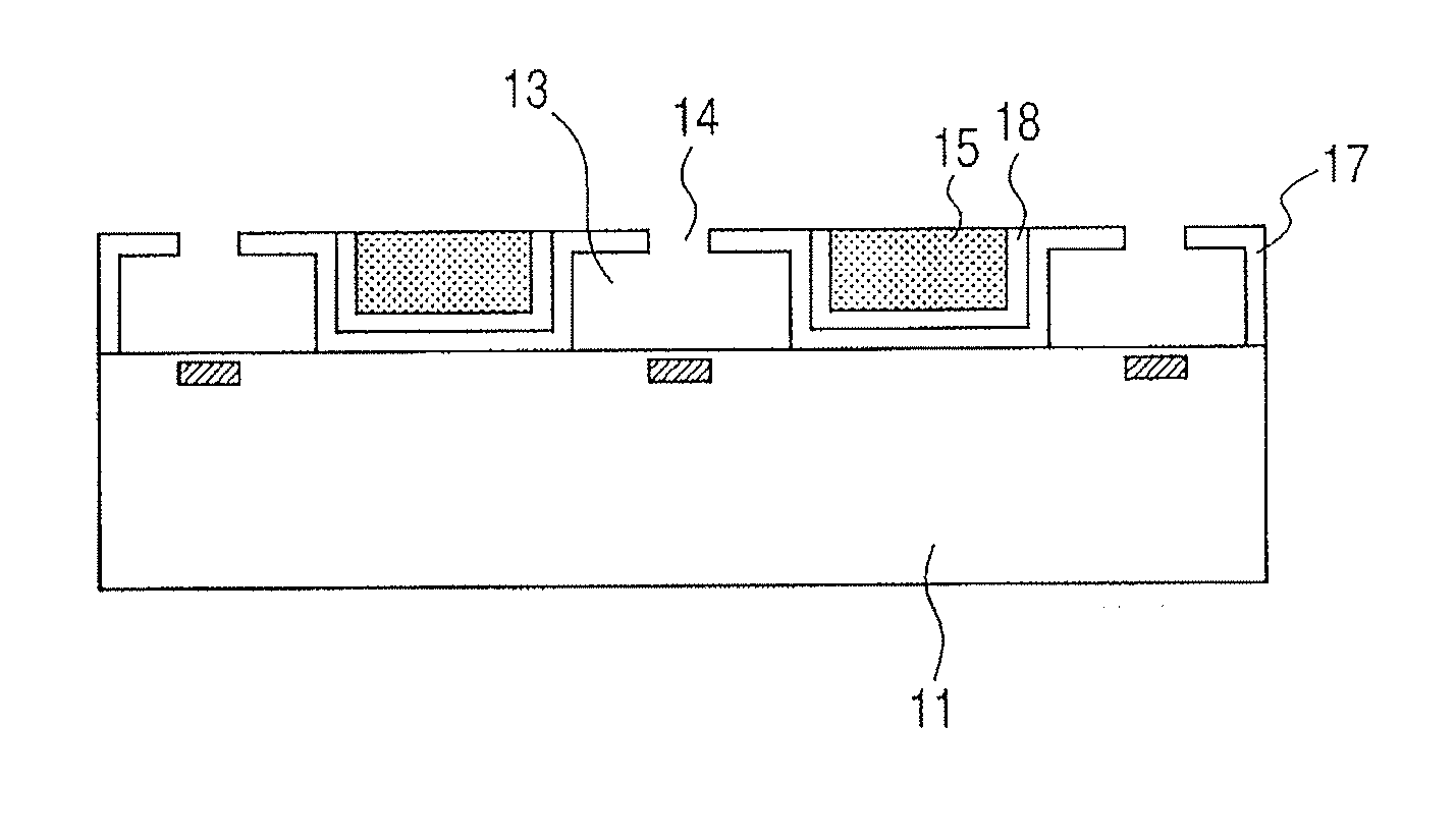
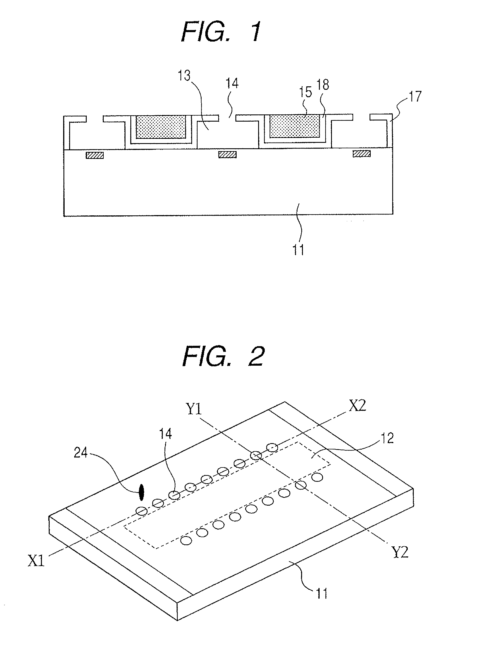
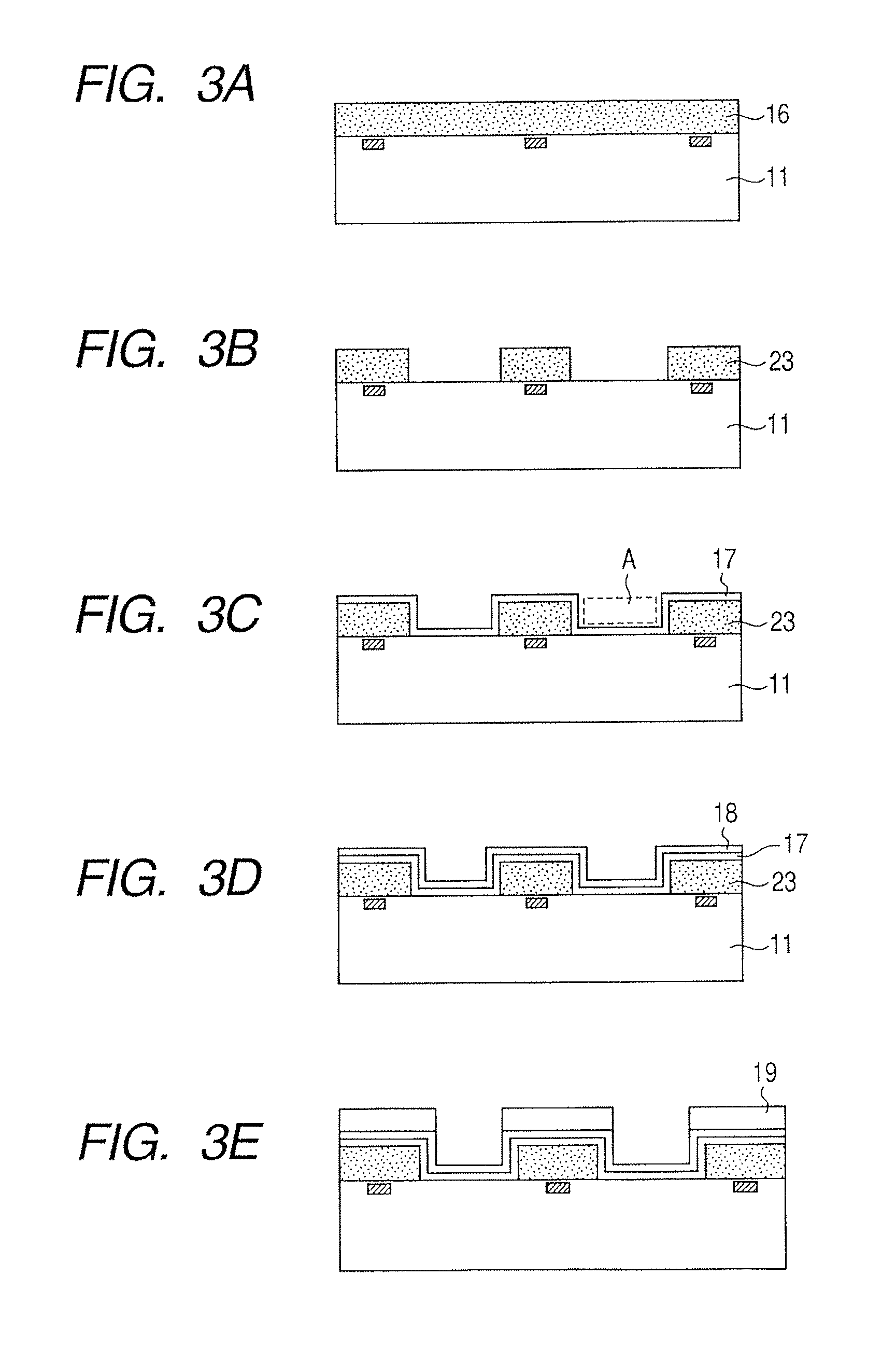
[0035]The process chart of FIGS. 3A, 3B, 3C, 3D, 3E, 3F, 3G, 3H, 3I and 3J is a schematic sectional view at the time of seeing the same surface as that of FIG. 1.

[0036]As shown in FIG. 3A, the substrate 11 on which heating resistors 18 as energy generating elements to generate energy to be used for discharging ink were formed was prepared. Next, Al 16 was formed on the substrate 11 to be about 15 μm in thickness by the sputtering method as a material to form the shapes of ink paths made of a removable material.

[0037]Next, as shown in FIG. 3B, resist was formed on the Al 16 by the photolithographic method, and the Al 16 was etched using the resist as a mask with phosphoric acid to form the shapes 23.

[0038]Next, as shown in FIG. 3C, a wall member 17 was formed to be 10 μm in thickness with silicon oxide by the CVD under the condition of about 400° C. using a mono-silane gas as a raw material. At this time, because the wall member 17 grew along the forms of the shapes 23, dent portions...

example 2

[0047]As for the present example, a description is given to an example forming surface protection films for protecting the surfaces in which the discharge ports are formed in addition to the structure of the example 1.

[0048]As shown in FIG. 3G, the manufacturing process was performed similarly to that of the example 1 until the step of flattening the surfaces of the shapes 23 and the metal layers 15.

[0049]A description is given to the steps after the flattening step.

[0050]FIGS. 5A, 5B, 5C and 5D are schematic sectional views pertaining to a cross-section similar to that of FIG. 1.

[0051]As shown in FIG. 5A, a layer 23 to become the surface protection film 22 was formed on the flattened surface formed of the metal layers 15, the wall member 17 and the undercoat layers 18.

[0052]Next, as shown in FIG. 5B, the resist 20 for forming the discharge ports was formed into a predetermined form by the photolithographic method.

[0053]Next, as shown in FIG. 5C, the surface protection films 22 were...

example 3

[0056]FIG. 6 is a schematic sectional view showing the ink jet recording head of example 3 according to the present invention, and is a view pertaining to the cross-section through the line Y1-Y2 in FIG. 2, which cross-section is perpendicular to the substrate. The example 3 is an example in which the metal layers existing between walls of adjacent ink paths are connected to the wiring for driving heating resistors to attain the decrease of electric resistance.

[0057]As shown in FIG. 6, there are heating resistors 103 that were built into a substrate 101 in advance, and wiring layers 104 connected to a driver for driving heating resistors 103. Metal layers 110 formed by plating are connected to the wiring layers 104. Moreover, a reference numeral 111 denotes a surface protection layer; a reference numeral 112 denotes a discharge port; and a reference numeral 113 denotes a supply port. Moreover, wall members for forming the metal layers 110 by plating are formed.

[0058]FIG. 8 is an ill...


PUM

PropertyMeasurementUnit
thicknessaaaaaaaaaa
thicknessaaaaaaaaaa
thicknessaaaaaaaaaa

Abstract

An ink jet recording head includes a substrate provided with an energy generating element to generate energy used for discharging ink, a discharge port through which the ink is discharged, a supply port for supplying the ink, and an ink path formed on the substrate for making the discharge port and the supply port communicate with each other, wherein wall members forming the ink path are made of an inorganic material, and a space between adjacent ink paths is filled up by a metal layer.

Description

BACKGROUND OF THE INVENTION[0001]1. Field of the Invention[0002]The present invention relates to an ink jet recording head performing recording by discharging ink and a manufacturing method thereof.[0003]2. Description of the Related Art[0004]The ink jet recording systems disclosed in U.S. Pat. No. 4,723,129 and U.S. Pat. No. 4,740,796 can perform high-speed, high-density, high-accuracy, high-image-quality recording, and are suitable for colorization and compactification. A recording head that uses the ink jet recording systems to bubble ink using thermal energy for discharging the bubbled ink onto a recording medium is generally configured as follows. That is, the configuration is one in which a heating resistor for bubbling the ink and wiring to perform electric connection to the heating resistor are produced on the same substrate to use the substrate as a substrate for an ink jet recording head and further nozzles for discharging the ink are formed over the substrate.[0005]On the...

Claims


Application Information

Patent Timeline
Patent Type & Authority Patents(United States)
IPC IPC(8): B41J2/05
CPCB41J2/1603B41J2/1628B41J2/1629B41J2/1642B41J2/1643B41J2/1646B41J2/1631Y10T29/49401
Inventor OZAKI, TERUOSAITO, ICHIROONO, KENJIIBE, SATOSHISAKAI, TOSHIYASUYOKOYAMA, SAKAISHIBATA, KAZUAKI
Owner CANON KK
Why Eureka
Try Eureka