Photoreceiver/amplifier circuit, optical pickup device, and optical disk device

a photoreceiver and amplifier technology, applied in the direction of amplifiers with semiconductor devices only, amplifiers with semiconductor devices/discharge tubes, amplifier modifications to reduce noise influence, etc., can solve the problems of increasing transistor shot-noise and noise assumably increasing, so as to achieve desirable offset characteristics and ensure noise reduction

Inactive Publication Date: 2011-01-11
SHARP KK
View PDF10 Cites 37 Cited by
  • Summary
  • Abstract
  • Description
  • Claims
  • Application Information

AI Technical Summary

Benefits of technology

[0044]With this arrangement in which a resistance of the feedback resistor is greater than a resistance of the reference resistor, the noise from a low-frequency band can be securely reduced. Besides, since the compensation circuit compensates a difference between the voltage between terminals of the feedback resistor and a voltage between terminals of the reference resistor, it is possible to prevent an offset voltage caused by the difference between the resistance of the feedback resistor and the resistance of the reference resistor.
[0055]An optical pickup device according to the present invention includes the photoreceiver / amplifier circuit having the foregoing structure, and therefore ensures noise reduction and improved offset voltage characteristic in a photoreceiver / amplifier circuit. With this advantage, particularly when converting reflection light from an optical disk into a signal voltage, the optical pickup device improves qualities of output signals. Further, an optical disk device according to the present invention includes the optical pickup device, and therefore improves qualities of output signals in the same manner.

Problems solved by technology

On the other hand, the photoreceiver / amplifier circuit disclosed in the foregoing laid-open patent publication increases a transistor shot-noise by using a n-times bias current of the controlling the offset adjustment circuit.
The noise assumably increases in this case.

Method used


Image

  • Photoreceiver/amplifier circuit, optical pickup device, and optical disk device
  • Photoreceiver/amplifier circuit, optical pickup device, and optical disk device
  • Photoreceiver/amplifier circuit, optical pickup device, and optical disk device

Examples


first embodiment

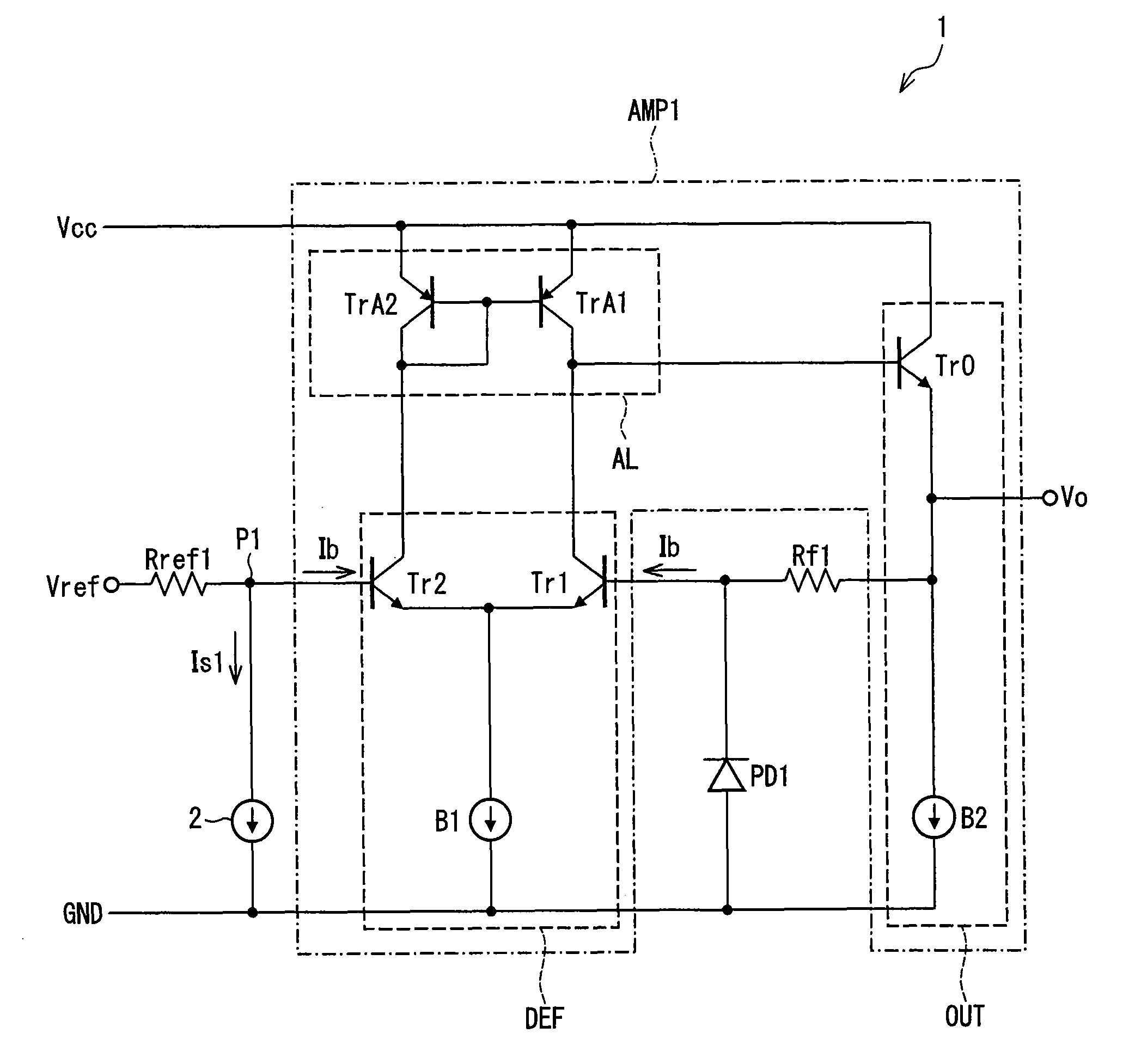
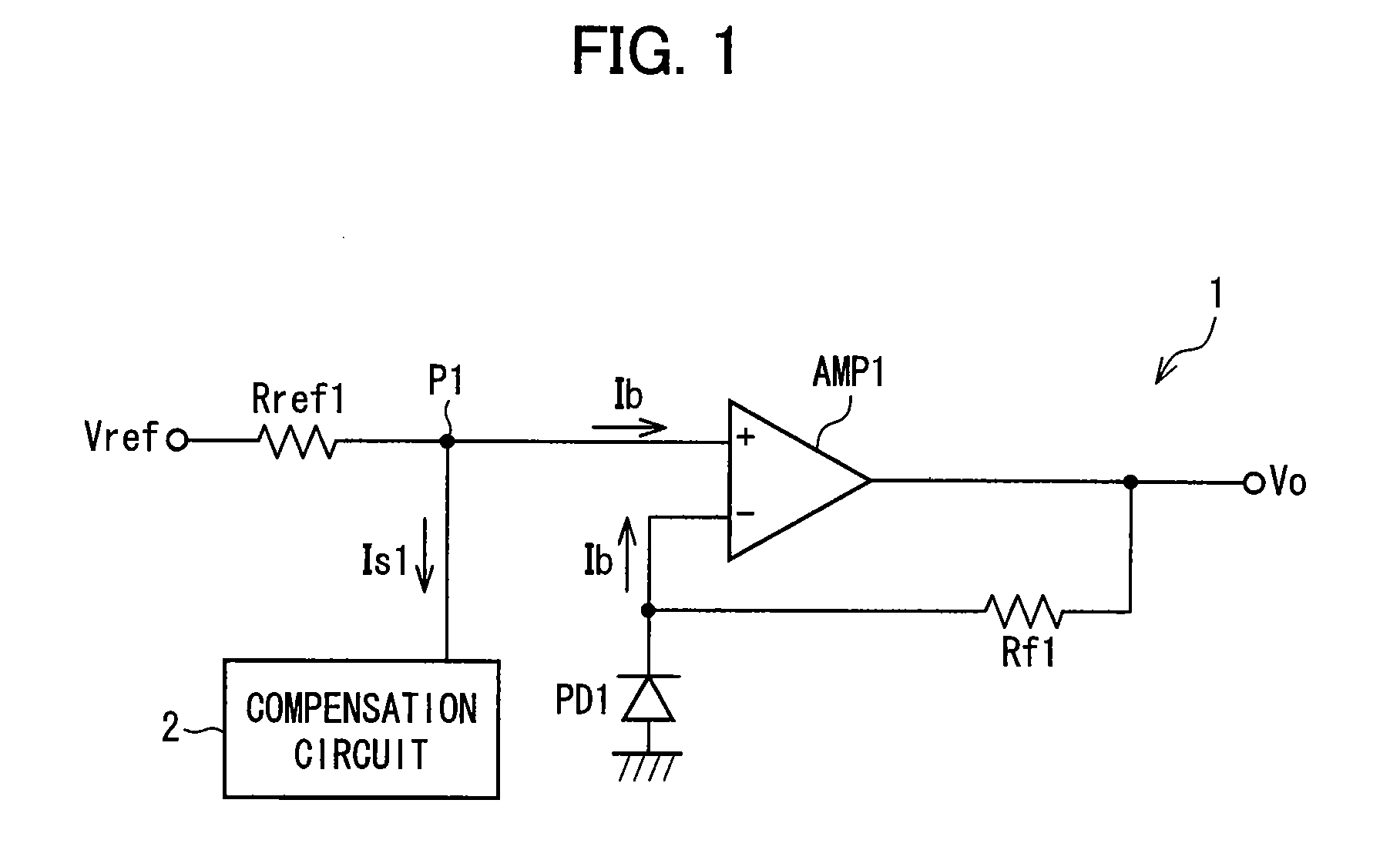
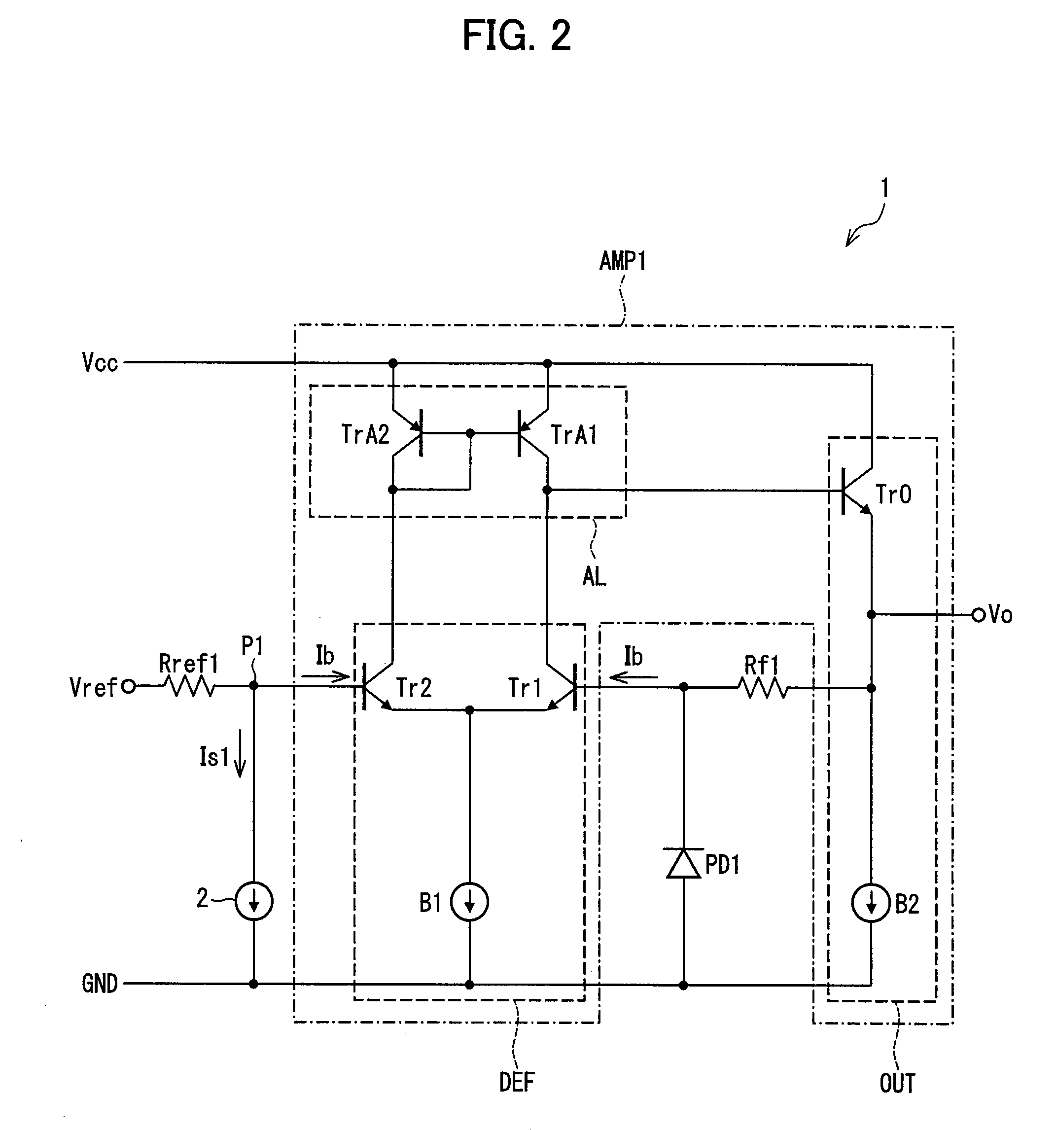
[0084]One embodiment of the present invention is described below with reference to FIGS. 1 to 3.

[0085]FIG. 1 shows a schematic structure of a photoreceiver / amplifier circuit 1 according to the present embodiment. FIG. 2 shows a circuit structure of the photoreceiver / amplifier circuit 1.

[0086]FIG. 3 shows a detailed circuit structure of the photoreceiver / amplifier circuit 1.

[0087]The photoreceiver / amplifier circuit 1 is used as each of the photoreceiver / amplifier circuits 101a to 101d shown in FIG. 17, and amplifies photocurrents generated in the photodiodes PDA to PDD of FIG. 16 by converting them into voltages. Note that, the photoreceiver / amplifier circuit according to the later described Second Embodiment is also used as each of the photoreceiver / amplifier circuits 101a to 101d.

[0088]As shown in FIG. 1, the photoreceiver / amplifier circuit 1 includes a photodiode PD1, a differential amplifier circuit AMP1, a feedback resistor Rf1, a reference resistor Rref1 and a compensation cir...

second embodiment

[0129]Another embodiment of the present invention is described below with reference to FIGS. 4 through 6. For ease of explanation, materials having the equivalent functions as those shown in the drawings pertaining to the foregoing First Embodiment will be given the same reference symbols, and explanation thereof will be omitted here.

[0130]FIG. 4 shows a schematic structure of a photoreceiver / amplifier circuit 11 according to the present embodiment. FIG. 5 shows a circuit structure of the photoreceiver / amplifier circuit 11. FIG. 6 shows a detailed circuit structure of the photoreceiver / amplifier circuit 11.

[0131]As shown in FIG. 5, the photoreceiver / amplifier circuit 11 includes a photodiode PD1, a differential amplifier circuit AMP1, a feedback resistor Rf1, and a reference resistor Rref1, as with the photoreceiver / amplifier circuit 1. However, the photoreceiver / amplifier circuit 11 includes a compensation circuit 12 instead of the compensation circuit 2.

[0132]Unlike the compensati...

third embodiment

[0156]Still another embodiment of the present invention is described below with reference to FIGS. 7 and 8. For ease of explanation, materials having the equivalent functions as those shown in the drawings pertaining to the foregoing First Embodiment will be given the same reference symbols, and explanation thereof will be omitted here.

[0157]FIG. 7 shows a circuit structure of a photoreceiver / amplifier circuit 20 according to the present embodiment. FIG. 8 shows a detailed circuit structure of the photoreceiver / amplifier circuit 20.

[0158]The photoreceiver / amplifier circuit 20 is used as each of the photoreceiver / amplifier circuits 101A to 101D shown in FIG. 20, and amplifies photocurrents generated in the photodiodes PDA to PDD and PDa to PDd of FIG. 19 by converting them into voltages. Note that, the photoreceiver / amplifier circuits according to the later described Fourth and Ninth Embodiments are also used as each of the photoreceiver / amplifier circuits 101A to 101D.

[0159]As shown...


PUM


Abstract

The subject invention provides a photoreceiver / amplifier circuit comprising a differential circuit including a differential transistor pair and a bias circuit; an active load; a feedback resistor for converting a photocurrent generated from a photodiode into a voltage; a reference resistor; and a compensation circuit. The resistance of the feedback resistor is greater than the resistance of the reference resistor. The compensation circuit supplies a compensation current from a junction between the feedback resistor and a non-inverting input terminal of the differential amplifier circuit, so as to cancel the difference between a voltage between terminals of the feedback resistor and a voltage between terminals of the reference resistor. This reduces noise and improves offset voltage characteristics. The present invention provides a photoreceiver / amplifier circuit ensuring noise reduction and desirable offset voltage characteristics.

Description

[0001]This Nonprovisional application claims priority under 35 U.S.C. §119(a) on Patent Application No. 2006 / 263542 filed in Japan on Sep. 27, 2006, and Patent Application No. 2007 / 181433 filed in Japan on Jul. 10, 2007, the entire contents of which are hereby incorporated by reference.FIELD OF THE INVENTION[0002]The present invention relates to a photoreceiver / amplifier circuit added to an optical receiver mounted to an optical pickup device which performs reproduction / recording of optical disks, particularly to a photoreceiver / amplifier circuit for amplifying a photocurrent signal from the optical receiver and converting it into a voltage. The present invention also relates to an optical disk device and an optical pickup device including the photoreceiver / amplifier circuit.BACKGROUND OF THE INVENTION[0003]Optical disks including DVDs and CDs are widely used as media for recording music, pictures, data information etc. Reproduction and recording of information from / to the media are...

Claims


Application Information

Patent Timeline
Patent Type & Authority Patents(United States)
IPC IPC(8): H03F3/08
CPCH03F1/26H03F3/087H03F3/45085H03F3/45475H03F3/456H03F3/45973H03F2203/45212H03F2203/45528H03F2203/45536H03F2203/45618
Inventor OHNISHI, MASAYA
Owner SHARP KK
Why Eureka
Try Eureka