Production process for surface-mounting ceramic LED package, surface-mounting ceramic LED package produced by said production process, and mold for producing said package

a production process and ceramic technology, applied in the field of surface-mounting ceramic led package production process, can solve the problems of attenuation of the amount of radiated light, interference of light radiated from a certain led chip, and mutual dimming, so as to reduce the emission rate, easy to produce, and good yield

Inactive Publication Date: 2011-01-18
EI DU PONT DE NEMOURS & CO
View PDF15 Cites 2 Cited by
  • Summary
  • Abstract
  • Description
  • Claims
  • Application Information

AI Technical Summary

Benefits of technology

[0017]According to the present production process of a ceramic LED package of the present invention, a ceramic LED package, in which decreases in emission rate caused by optical interference can be avoided even in the case of having a plurality of LED chips, can be easily produced at good yield.

Problems solved by technology

However, when a plurality of LED chips is placed inside the same concave portion, there was the problem of light radiated from a certain LED chip being interfered with by the light from an adjacent LED chip.
Since light radiated from the sides of a chip opposes light radiated from an adjacent chip, radiated light of different wavelengths interfere causing the light to be mutually diminished.
This results in problems of attenuation of the amount of radiated light and the occurrence of unevenness in the amount of light.
Since plastic may be deteriorated by ultraviolet rays contained in light emitted from LED chips, it is not optimal for use in LED packages.
In addition, although high-output LED chips emit radiated light of high brightness, the amount of heat dissipated also increases.
Since plastic packages lack heat resistance, thermal deterioration is considerable thereby resulting in the problem of a short service life of the package itself.
On the other hand, although ceramic packages have superior heat resistance, they had the problem of being inferior to the mold ability of plastic products with respect to fine structures such as inclined or curved radiated light reflecting surfaces or partitions between chips.
For this reason, ceramic packages have difficulty in guiding light radiated from an LED chip in a desired direction, ultimately resulting in a loss in the amount of radiated light.

Method used


Image

  • Production process for surface-mounting ceramic LED package, surface-mounting ceramic LED package produced by said production process, and mold for producing said package
  • Production process for surface-mounting ceramic LED package, surface-mounting ceramic LED package produced by said production process, and mold for producing said package
  • Production process for surface-mounting ceramic LED package, surface-mounting ceramic LED package produced by said production process, and mold for producing said package

Examples


first embodiment

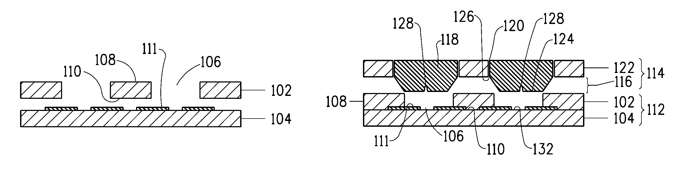
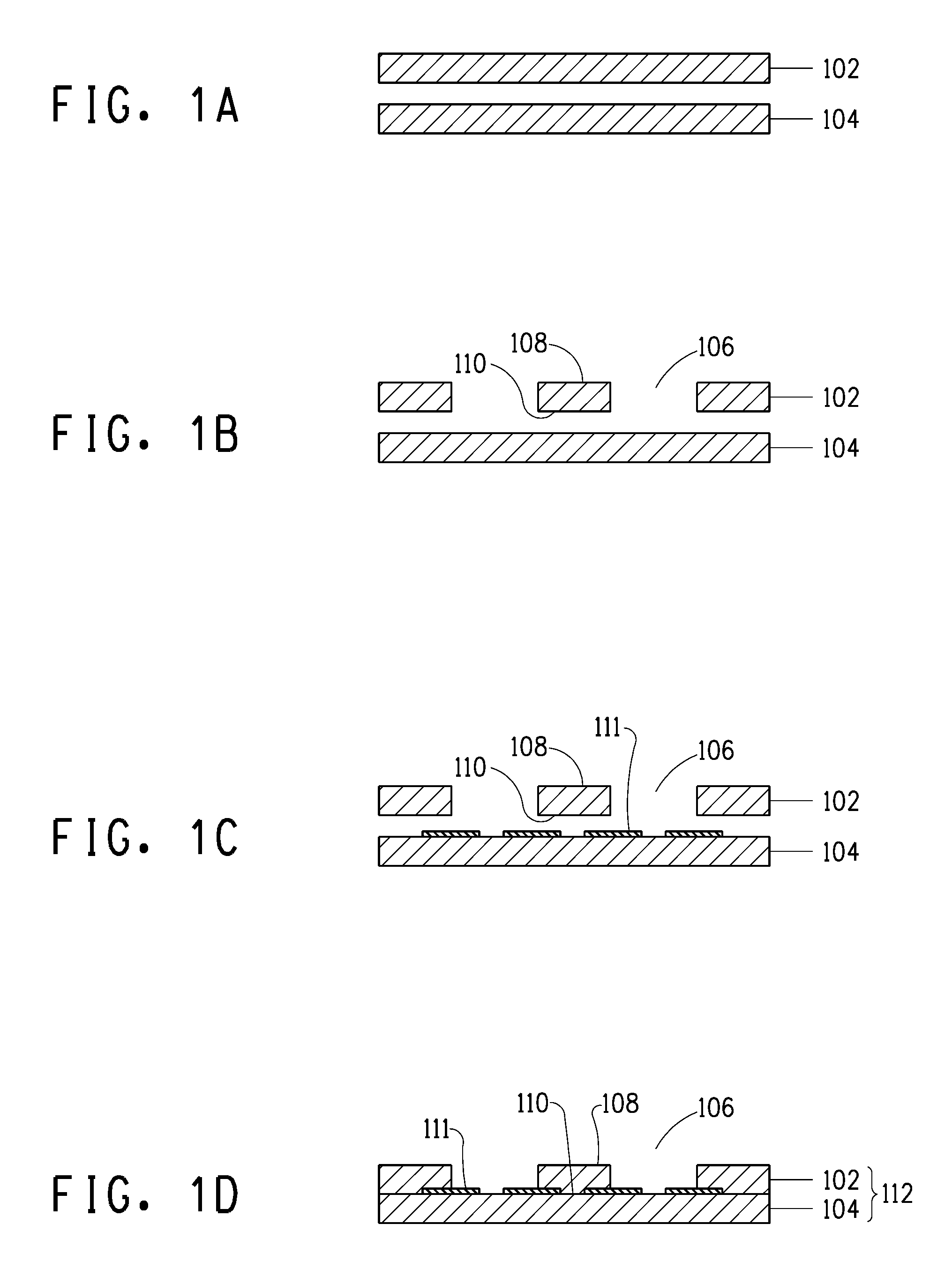
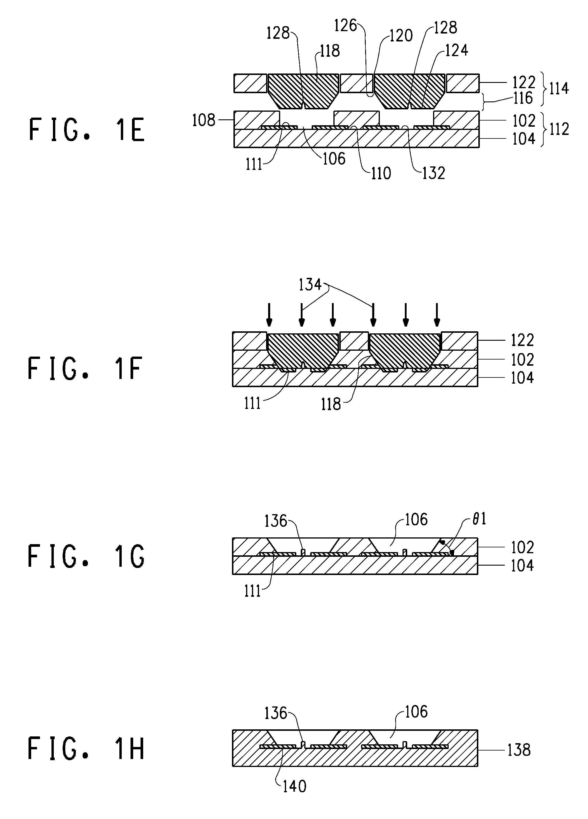
[0034]A first aspect of the present invention is a production process of a surface-mounting ceramic LED package. A first embodiment of this production process comprises the following steps:[0035](i) preparing a first ceramic green sheet and a second ceramic green sheet, and forming through holes in the first ceramic green sheet,[0036](ii) forming LED connection electrodes in the first and / or second ceramic green sheet,[0037](iii) layering the first ceramic green sheet and the second ceramic green sheet to form a ceramic green sheet substrate having a convex portion,[0038](iv) inserting a mold, which comprises a base portion that presses portions other than the concave portion of the first ceramic green sheet of the ceramic green sheet substrate, and an insertion portion having a convex portion that protrudes from the base portion and presses the inside of the concave portion of the ceramic green sheet substrate, into the concave portion of the ceramic green sheet substrate so that t...

second embodiment

[0131]The following provides an explanation of an example of a second embodiment of the ceramic LED package according to FIGS. 9 and 10.

[0132]FIG. 9A is an overhead view of a ceramic LED package 700, while FIG. 9B is a cross-sectional view taken along line 9B of FIG. 9A. In addition, FIG. 9C shows a ceramic LED package mounted with LED chips (ceramic LED device). FIGS. 10A and 10B are drawings showing examples of the shapes of the electrodes of the ceramic LED package of the second embodiment. Furthermore, a description of the electrodes is omitted in FIG. 9.

[0133]In this embodiment, the ceramic LED package 700 has a ceramic substrate 138, a concave portion 304 formed in roughly the center thereof, and a partition 702 provided in the bottom 306 of the concave portion. The shape of the lateral surface 310 of the concave portion 304, the inclination angle (θ1) and other characteristics are the same as in the first embodiment.

[0134]There are no particular limitations on the shape of th...

third embodiment

[0141]The following provides an explanation of an example of a ceramic LED package of a third embodiment according to FIGS. 11 and 12. FIG. 11A is an overhead view of a ceramic LED package 900, while FIG. 11B is a cross-sectional view taken along line 11B of FIG. 11A. In addition, FIG. 11C shows a ceramic LED package mounted with LED chips (ceramic LED device). FIGS. 12A and 12B are drawings showing examples of the shapes of electrodes of the ceramic LED package of the third embodiment. Furthermore, a description of the electrodes is omitted in FIG. 11.

[0142]In this embodiment, the ceramic LED package 900 has a ceramic substrate 138, a concave portion 304 formed in roughly the center thereof, and partitions 902 and 904 provided in the bottom 306 of the concave portion. The shape of the lateral surface 310 of the concave portion 304, the inclination angle (θ1) and other characteristics are the same as in the first embodiment.

[0143]There are no particular limitations on the shape of t...


PUM

PropertyMeasurementUnit
sizeaaaaaaaaaa
thicknessaaaaaaaaaa
thicknessaaaaaaaaaa

Abstract

The present invention is related to a surface-mounting ceramic LED package and a method for its production comprising: layering a ceramic green sheet which has a hole and a second ceramic green sheet, inserting a mold with a groove to form a partition in the bottom of the ceramic green sheet substrate, and firing the ceramic green sheet substrate.

Description

BACKGROUND OF THE INVENTION[0001]1. Field of the Invention[0002]The present invention relates to a production process for a surface-mounting ceramic light emitting diode (LED) package, a surface-mounting ceramic LED package produced by the production process, and a mold for producing the package.[0003]2. Technical Background[0004]LEDs are widely applied as backlighting for displays and light sources for general illumination and the like. LED packages can be broadly classified into dome packages and surface-mounting packages. In the case of the dome LED packages, an LED chip is mounted to a lead frame and the periphery thereof is molded into the shape of a dome with resin. The reason for molding the resin into the shape of a dome is to focus the light from the chip forward by refraction, thereby improving the amount of radiated light. In the case of the surface-mounting packages, an LED chip is placed in the bottom of a recess in a concave board and sealed with resin. Since surface-m...

Claims


Application Information

Patent Timeline
Patent Type & Authority Patents(United States)
IPC IPC(8): H01L21/00H01L51/00H01L29/26H01L27/15
CPCH01L25/0753H01L33/486H01L33/60H01L2924/09701H01L2224/48091H01L2924/00014H01L33/48H01L33/52H01L33/62
Inventor NAKAJIMA, NAOTOTSUNODA, SHUICHIINABA, AKIRA
Owner EI DU PONT DE NEMOURS & CO
Why Eureka
Try Eureka