
Liquid crystal panel substrate, liquid crystal panel, and electronic device and projection display device using the same

a technology of liquid crystal panels and substrates, applied in semiconductor devices, optics, instruments, etc., can solve the problems of affecting the appearance quality of liquid crystal substrates, so as to achieve effective suppression of variations of liquid crystal refractive indexes and improve image quality , the effect of improving the reliability of the liquid crystal substra

Inactive Publication Date: 2011-01-18
SEIKO EPSON CORP
View PDF73 Cites 20 Cited by
  • Summary
  • Abstract
  • Description
  • Claims
  • Application Information

AI Technical Summary

Benefits of technology

[0010]It is an object of the present invention to provide a reflective liquid crystal panel substrate and a liquid crystal panel having a passivation film which does not vary the refractive index of the liquid crystal and having high reliability.
[0011]It is another object of the present invention to provide a reflective liquid crystal panel having high reliability and excellent image quality and an electronic device and projection display device using the same.
[0012]The present invention for achieving the above object has a liquid crystal panel substrate comprising a matrix of reflective electrodes formed on a substrate, a transistor formed corresponding to each reflective electrode, a voltage applied to the reflective electrodes through the respective transistors, a passivation film formed on the reflecting electrodes, the passivation film having a thickness to control a change in reflectance of the reflecting electrodes to wavelengths of incident light to within approximately 1%, and thus the thickness is selected such that the variation of the thickness less affects the reflectance of the reflecting electrodes.

Problems solved by technology

In transmissive liquid crystal panels, since the switching element-forming region, such as a TFT, which is provided in each pixel is not a transparent region, it has a serious defect that the aperture ratio is low and decreases as the resolution of the panel is improved to XGA, or S-VGA.
Accordingly, the reflective liquid crystal panel has disadvantages, e.g. the reflectance noticeably varies with variation of the thickness of the passivation film.

Method used


Image

  • Liquid crystal panel substrate, liquid crystal panel, and electronic device and projection display device using the same
  • Liquid crystal panel substrate, liquid crystal panel, and electronic device and projection display device using the same
  • Liquid crystal panel substrate, liquid crystal panel, and electronic device and projection display device using the same

Examples


Embodiment Construction

[0038]Preferred embodiments in accordance with the present invention will now be described with reference to the drawings.

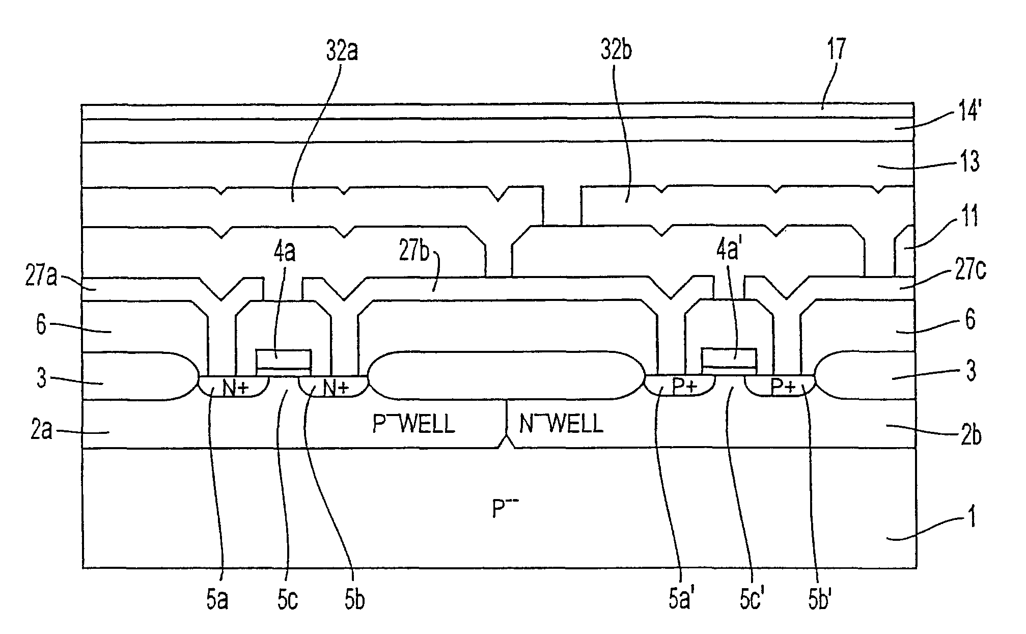
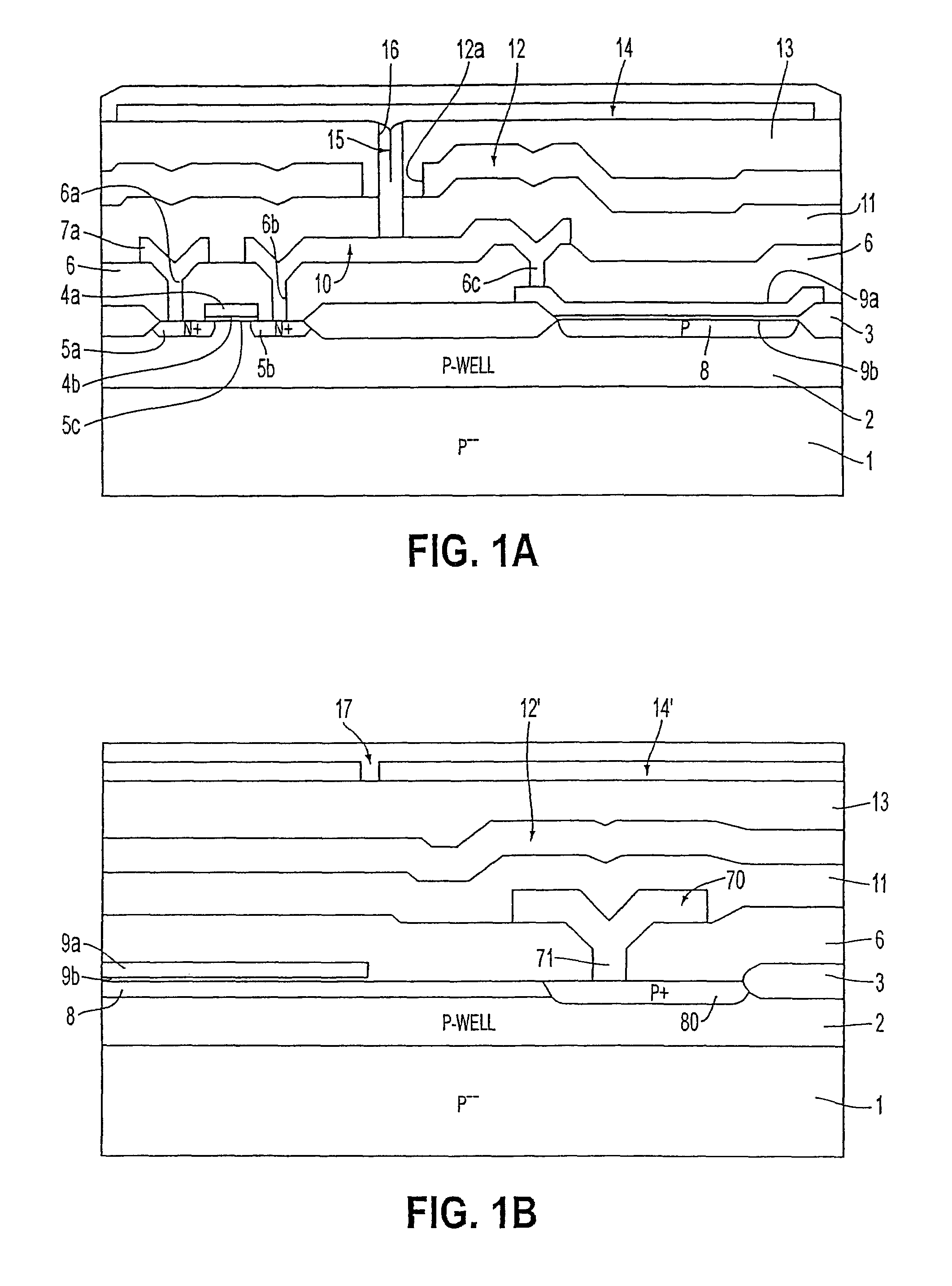
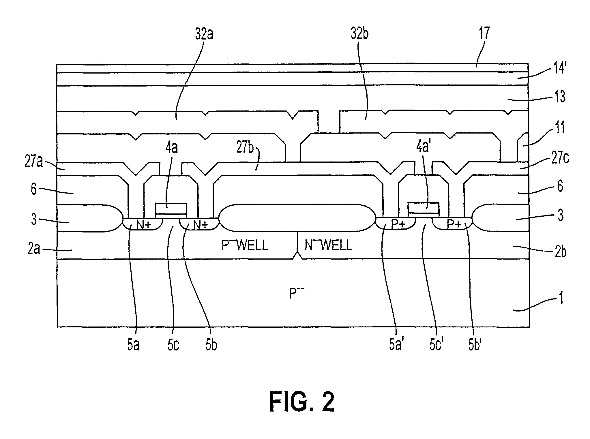
[0039]FIGS. 1(a), 1(b) and 3 show a first embodiment of a reflecting electrode substrate of a reflective liquid crystal panel in accordance with the present invention. FIGS. 1(a), 1(b) and 3 are a cross-sectional view and a planar layout view, respectively, of one pixel section among a matrix of pixels. FIG. 1(a) is a cross-sectional view taken along cross-section line I-I of FIG. 3. FIG. 1(b) is a cross-sectional view taken along cross-section line II-II of FIG. 3. FIG. 6 is an entire planar layout view of a reflecting electrode substrate of a reflective liquid crystal panel in accordance with the present invention.

[0040]In FIGS. 1(a) and 1(b), identification numeral 1 represents a P-type semiconductor substrate such as single-crystal silicon for N-type semiconductor substrate (N−−)), identification numeral 2 represents a P-type well region having an impurity co...


PUM

PropertyMeasurementUnit
reflectanceaaaaaaaaaa
thicknessaaaaaaaaaa
thicknessaaaaaaaaaa

Abstract

In a liquid crystal substrate in which a matrix of reflecting electrodes is formed on a substrate, a transistor is formed corresponding to each reflective electrode and a voltage is applied to the reflective electrode through the transistor. A silicon oxide film having a thickness of 500 to 2,000 angstroms is used as the passivation film and the thickness is set to a value in response to the wavelength of the incident light to maintain a substantially constant reflectance.

Description

[0001]This is a Continuation of application Ser. No. 12 / 382,926, filed Mar. 26, 2009, which in turn is a Continuation of Ser. No. 11 / 987,379, filed Nov. 29, 2007, granted on May 12, 2009 as U.S. Pat. No. 7,532,292, which is in turn a Continuation of application Ser. No. 11 / 477,645, filed Jun. 30, 2006, granted on Jan. 28, 2008 as U.S. Pat. No. 7,324,171, which in turn is a Divisional of application Ser. No. 11 / 378,252, filed Mar. 20, 2006, granted on Feb. 27, 2007 as U.S. Pat. No. 7,184,105, which in turn is a Continuation of application Ser. No. 11 / 152,163, filed Jun. 15, 2005, granted on Jan. 2, 2007 as U.S. Pat. No. 7,158,205, which in turn is a Divisional of application Ser. No. 10 / 021,012, filed Dec. 19, 2001, granted on Aug. 23, 2005 as U.S. Pat. No. 6,933,996, which in turn is a Divisional of application Ser. No. 08 / 955,461, filed Oct. 21, 1997, granted on Feb. 5, 2002 as U.S. Pat. No. 6,344,888. The disclosures of the prior applications are hereby incorporated by reference h...

Claims


Application Information

Patent Timeline
Patent Type & Authority Patents(United States)
IPC IPC(8): G02F1/1333G02F1/1335G02F1/136
CPCG02F1/13454G02F1/136209G02F1/1313G02F1/1368H01L33/08G02F1/1362G02F1/133345G02F2203/02H01L2924/0002H01L2924/00
Inventor YASUKAWA, MASAHIRO
Owner SEIKO EPSON CORP
Learn More