Plated ground features for integrated lead suspensions

Active Publication Date: 2011-01-25
HUTCHINSON TECH
View PDF16 Cites 55 Cited by
  • Summary
  • Abstract
  • Description
  • Claims
  • Application Information

AI Technical Summary

Benefits of technology

[0007]The present invention is a method for forming high-quality electrical interconnects on an integrated lead suspension or suspension component of the type having a spring metal layer, a conductive lead layer, and an insulator layer separating portions of the spring metal and conductive lead layers. An aperture is formed through only the insulator layer to expose the spring metal layer at an interconnect site

Problems solved by technology

Creating a good connection between the epoxy material and the stainless steel surface of the suspension assembly, however, has proven to be difficult because the stainless steel surface often has an adhered layer of oxidation on its surface, which prevents a good electrical connection.
Unfortunately, the circuit board

Method used


Image

  • Plated ground features for integrated lead suspensions
  • Plated ground features for integrated lead suspensions
  • Plated ground features for integrated lead suspensions

Examples


first embodiment

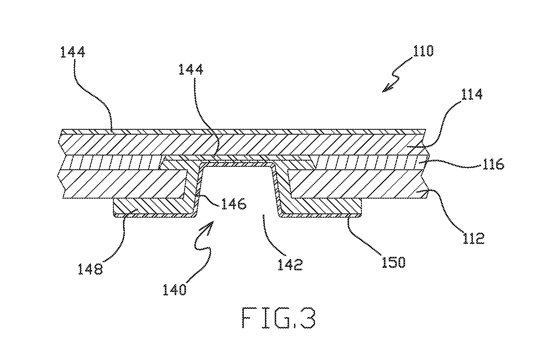
[0029]FIGS. 3, 4 and 5 are illustrations of an interconnect 140 in accordance with the present invention formed on the side of the spring metal layer 112 of flexure 110 (i.e., a “stainless steel side” interconnect). With the exception of interconnect 140, flexure 110 can be identical to flexure 10 described above, and similar reference numerals are used to identify corresponding features. As shown, the interconnect 140 is formed in an aperture 142 through the spring metal layer 112 and the insulator layer 116. The portion of aperture 142 extending through the insulator layer 116 is larger in diameter than the portion of the aperture extending through the spring metal layer 112 in the illustrated embodiment, but can be larger or smaller than the portion of the aperture through the spring metal layer in other embodiments. In the embodiment shown in FIG. 3, the surface of the conductor layer 114 exposed by the aperture 142 is plated with a relatively non-corrosive conductive material s...

second embodiment

[0030]FIGS. 6, 7 and 8 are illustrations of an interconnect 240 in accordance with the present invention formed on the side of the conductor layer 214 of flexure 210 (i.e., a “copper side” interconnect). With the exception of interconnect 240, flexure 210 can be identical to flexure 10 described above, and similar reference numerals are used to identify corresponding features. As shown, the interconnect 240 is formed in an aperture 242 through the conductor layer 214 and the insulator layer 216. The portion of aperture 242 extending through the insulator layer 216 is larger in diameter than the portion of the aperture extending through the conductor layer 214 in the illustrated embodiment, but can be larger or smaller than the portion of the aperture through the conductor layer in other embodiments. In the embodiment shown in FIG. 6, the surface of the conductor layer 214 exposed by the aperture 242, as well as other exposed surfaces of the conductor layer, are plated with a relativ...

third embodiment

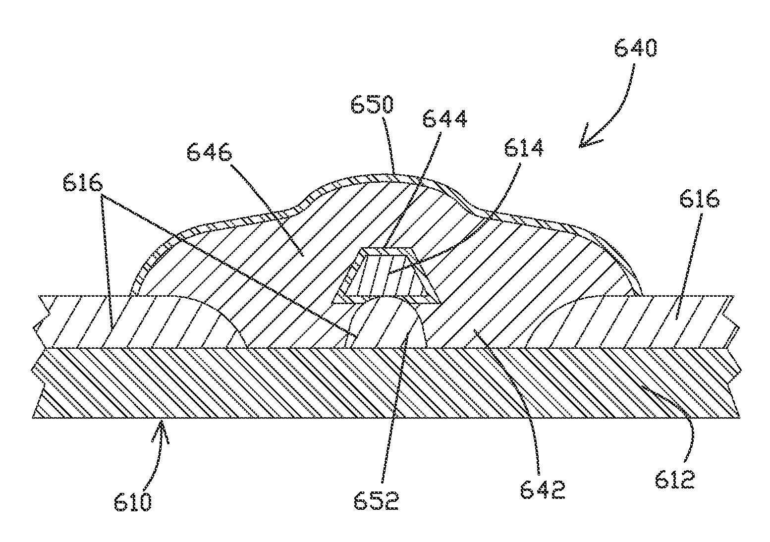
[0032]FIGS. 11-13 are illustrations of a bond pad interconnect 440 in accordance with the present invention formed on the side of the conductor layer 414 of flexure 410. With the exception of interconnect 440, flexure 410 can be identical to flexure 310 described above, and similar reference numerals are used to identify corresponding features. As shown, the bond pad interconnect 440 is formed in a gap or aperture 442 extending through the insulator layer 416 at the location of interconnect 440. An electroplated nickel or other conductive material interconnect plating 446 is built up or plated up over the spring metal layer 412 in the area of the aperture 442 corresponding to the desired location of the bond pad interconnect 440. As perhaps best shown in FIG. 11, the plating 446 of bond pad interconnect 440 is preferably built up to a height that is generally the same as the height of the other bond pads 424 on the flexure 410. The interconnect 440 is shaped to the desired size. As ...


PUM


Abstract

A method for forming an electrical interconnect on an integrated lead suspension or suspension component of the type having a stainless steel layer, a conductive lead layer and an insulator layer separating the stainless steel and conductive lead layers. An aperture is formed through only the insulator layer to expose the stainless steel layer at an interconnect site. An interconnect mask is applied around the interconnect site. A first conductive material is electroplated onto the stainless steel layer at the interconnect site to form a plated interconnect between the spring metal layer and the conductive lead layer. The mask is then removed. An electrical interconnect between the stainless steel and conductive lead layers including an aperture only through the insulator layer and an electroplated conductive material interconnect extending between both the spring metal layer and the conductive lead layer.

Description

FIELD OF THE INVENTION[0001]The invention relates generally to integrated lead or wireless suspensions for disk drive assemblies. In particular, the invention is an electrical interconnect such as a ground feature formed on the integrated lead suspensions.BACKGROUND OF THE INVENTION[0002]Integrated lead or wireless suspensions and flexures (i.e., suspension components) are used to support read / write transducers in disk drives or other dynamic data storage systems. These devices typically have a stainless steel or other spring metal layer for supporting the electrical traces. A layer of dielectric insulating material separates the traces from the stainless steel.[0003]Electrical connections between otherwise isolated conductors on suspension assemblies (e.g., between the conductor and stainless steel layers) can be created by applying a conductive epoxy material into a via or through hole extending through at least some of the layers. This interconnect can be formed using a screen pr...

Claims


Application Information

Patent Timeline
IPC IPC(8): H05K1/00
CPCG11B5/484H05K3/44G11B5/4853H05K1/056H05K3/244H05K3/421H05K2201/0347H05K2201/0367H05K2201/09554H05K2201/0969H05K2203/1184
Inventor TRONNES, JEFFREY M.DECKER, CEDARHAUGEN, BRETT L.
Owner HUTCHINSON TECH
Why Eureka
Try Eureka