Liquid crystal device

a liquid crystal device and liquid crystal technology, applied in the field of liquid crystal devices, can solve the problems of long field-off time mentioned above, not solved, shortening the switching time of the display operating in ips-mode for generating high-quality moving images, etc., and shortening the fall time of the electro-optic response. , the effect of fast in-plane switching

Inactive Publication Date: 2011-01-25
KOMITOV LACHEZAR
View PDF13 Cites 3 Cited by
  • Summary
  • Abstract
  • Description
  • Claims
  • Application Information

AI Technical Summary

Benefits of technology

[0015]A general object of the present invention is to alleviate the above problems and provide an improved liquid crystal device. In particular, an object of the invention is to provide a liquid crystal device having the capability of generating high contrast and wide viewing angle images and exhibiting a fast in-plane switching, more particularly to shorten the fall time of the electro-optic response, and hence to reduce the total switching time enabling a satisfactory display of moving images.

Problems solved by technology

Nonetheless, the switching time of the displays operating in IPS-mode is not short enough for generating high quality moving images.
However, also in these so-called fringe field switching (FFS) devices, dielectric coupling is generally utilised and the problem with the long field-off time mentioned above is thus not solved.
Furthermore, the required voltages are rather high.

Method used


Image

  • Liquid crystal device
  • Liquid crystal device
  • Liquid crystal device

Examples


example 1

Cell Comprising Bulk Layer with Hybrid Alignment (HAN) and Interdigitated Electrodes

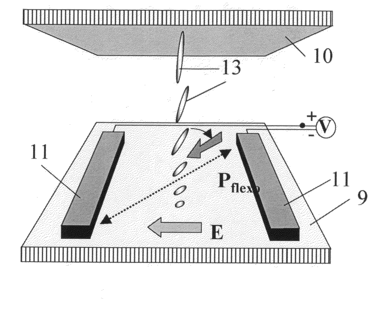
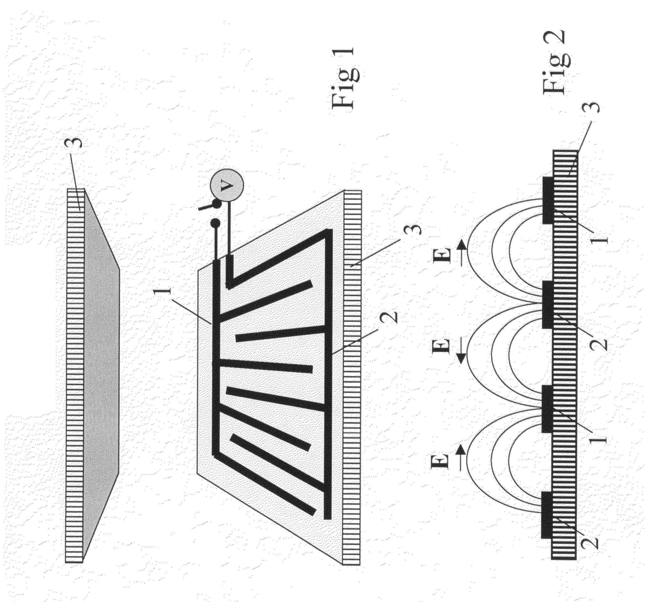
[0128]A sandwich cell (FIG. 20) comprising two parallel glass substrates 9 and 10 forming a cell gap of about 2 μm was used. An interdigitated electrode pattern 11 (illustrated in FIG. 1) were provided on the inner surface of one of the substrates 9 (single-sided device). The distance between adjacent electrodes was about 20 μm.

[0129]A first alignment layer 12 consisting of Nissan SE-2170 was deposited on the electrode pattern 11 and rubbed parallel to the electrode pattern 11 for promoting an uniform planar alignment of a liquid crystal bulk layer, comprising liquid crystal molecules 13, provided in the cell gap.

[0130]A second alignment layer 14 consisting of Nissan SE1211, promoting homeotropic alignment, was deposited on the inner surface of the other substrate 10.

[0131]The cell gap was filled with the nematic liquid crystalline material MLC 16000-000 (supplied by Merck) possessing positive dielec...

example 2

Cell Comprising Bulk Layer with Hybrid Alignment (HAN) and Interdigitated Electrodes

[0136]The same type of sandwich cell was used in this example as in the Example 1, but the HAN texture was reversed (FIG. 26). Thus, the alignment induced by the first alignment layer 18 at the substrate 15 bearing the electrode pattern 17 was homeotropic and the alignment induced by the second alignment layer 20 at the counter substrate 16 was planar, as shown in the FIG. 26 and FIG. 27.

[0137]In addition, the cell was filled with another nematic liquid crystalline material 19, MDA-05-187 (supplied by Merck) possessing a negative dielectric anisotropy (Δ∈<0.

[0138]Since the bend deformation is localized at the sub-strate 15 bearing the electrode pattern 17 and since MDA-05-187 exhibits a negative dielectric anisotropy, the strongest flexoelectric polarization (Pflexo) is here localized where the bend deformation is dominant, i.e. at the substrate 15 bearing the electrode pattern 17 (FIG. 26). The doub...

example 3

Cell Comprising Chiral Smectic Alignment Layer and Interdigitated Electrodes

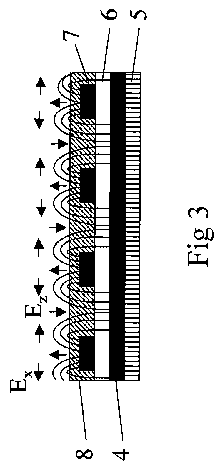
[0140]The cell used in this example (FIG. 32) had the same structure as the one used in Example 1. However, in this example, both inner surfaces of the substrates 21 and 22 were coated with alignment layers (not shown) comprising Nissan SE-2170 unidirectionally rubbed along the electrodes 23 promoting a quasi-planar alignment with pretilt θa.

[0141]On top of the alignment layer covering the electrode pattern 23, a thin film of ferroelectric liquid crystal polymer (FLCP), more specifically a ferroelectric side-chain polysiloxane, (not shown) was deposited. The FLCP layer had a molecular tilt θb and was aligned in bookshelf geometry, i.e. with smectic layers perpendicular to the substrate surface 21.

[0142]The cell gap was filled with an in-house prepared nematic liquid crystalline material 24 possessing a negative dielectric anisotropy (Δ∈<0) and being immiscible (insoluble) in the FLCP.

[0143]The applied electr...


PUM

PropertyMeasurementUnit
apex angleaaaaaaaaaa
angleaaaaaaaaaa
distanceaaaaaaaaaa

Abstract

The present invention relates to a liquid crystal device driven by a linear coupling, such as ferroelectric and / or flexoelectric coupling, between an inhomogenous in-plane electric field generated by an electrode pattern over a first sub-volume of the bulk layer adjacent to said electrode pattern and liquid crystals in a polarized state comprised in said first sub-volume and / or in an optional alignment layer applied on said electrode pattern said polarization being stronger than any possible similar liquid crystal polarization of the bulk layer outside said first sub-volume, said alignment layer, and / or a second sub-volume of the bulk layer adjacent the inner surface of the other substrate, or an optional second alignment layer or an optional electrode pattern applied thereon.

Description

TECHNICAL FIELD[0001]The present invention generally relates to the field of liquid crystals. More specifically, the present invention relates to a liquid crystal device driven by a linear coupling, such as ferroelectric and / or flexoelectric coupling, between liquid crystals in a polarized state and an applied in-plane electric field.TECHNICAL BACKGROUND[0002]In general, nematic liquid crystal displays (LCD) are operating on the basis of dielectric coupling, i.e. the coupling between dielectric anisotropy (Δ∈) of the liquid crystal and an applied electric field which gives rise to an electro-optic response. This response is quadratic with the applied field, i.e. it is not polar, and arises from the switching of the liquid crystal molecules by the field. In conventional nematic LCDs, the switching of the liquid crystal molecules takes place in a plane containing the direction of the applied electric field which means that an electric field applied across a liquid crystal sandwich cel...

Claims


Application Information

Patent Timeline
Patent Type & Authority Patents(United States)
IPC IPC(8): G02F1/133
CPCG02F1/133707G02F1/134363G02F1/133377G02F1/141
Inventor KOMITOV, LACHEZAR
Owner KOMITOV LACHEZAR
Why Eureka
Try Eureka