Simultaneous sample manipulation and sensing using surface acoustic waves
a surface acoustic wave and sample manipulation technology, applied in generators/motors, instruments, specific gravity measurements, etc., can solve the problems of non-specifically bound (nsb) protein interactions that interfere with sensor response and concentration determination, exaggerated response, false respons
- Summary
- Abstract
- Description
- Claims
- Application Information
AI Technical Summary
Benefits of technology
Problems solved by technology
Method used
Image
Examples
example 1
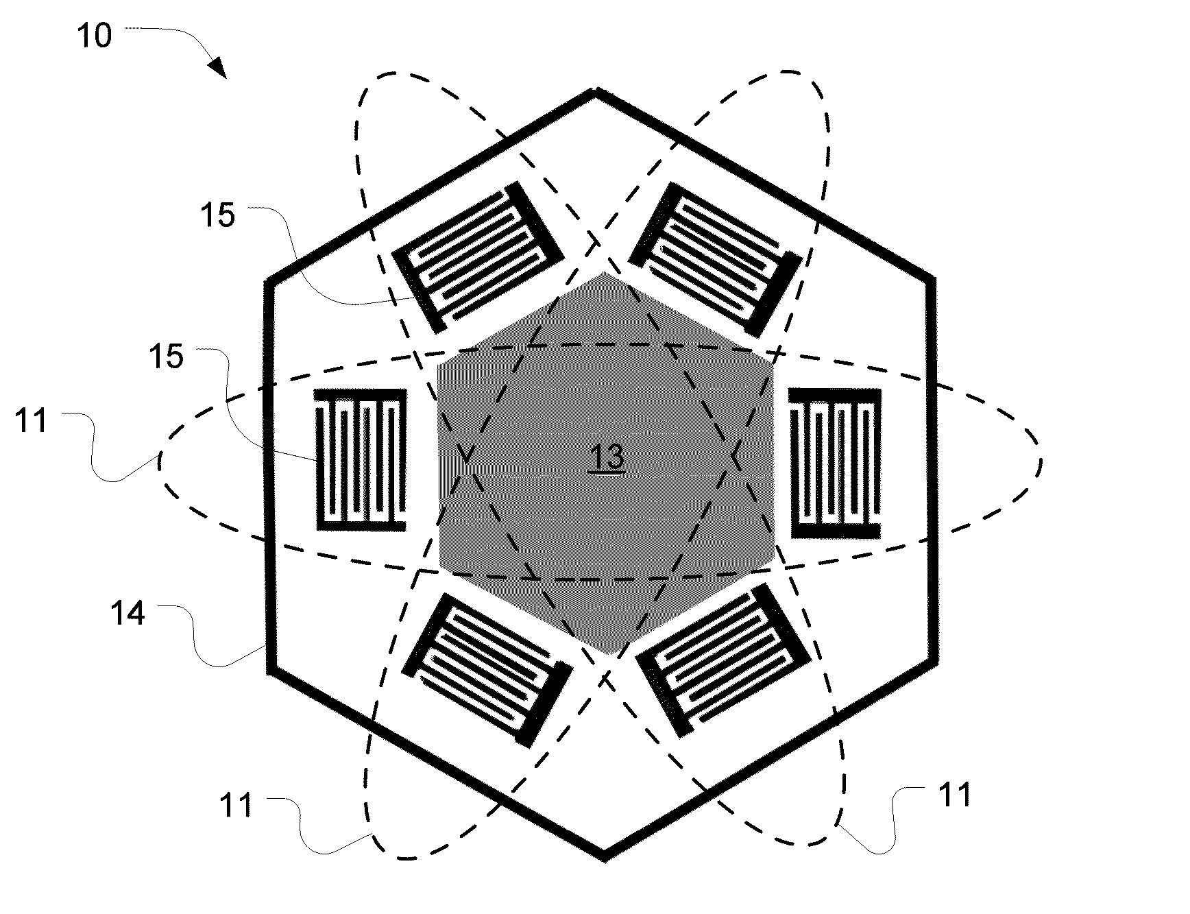
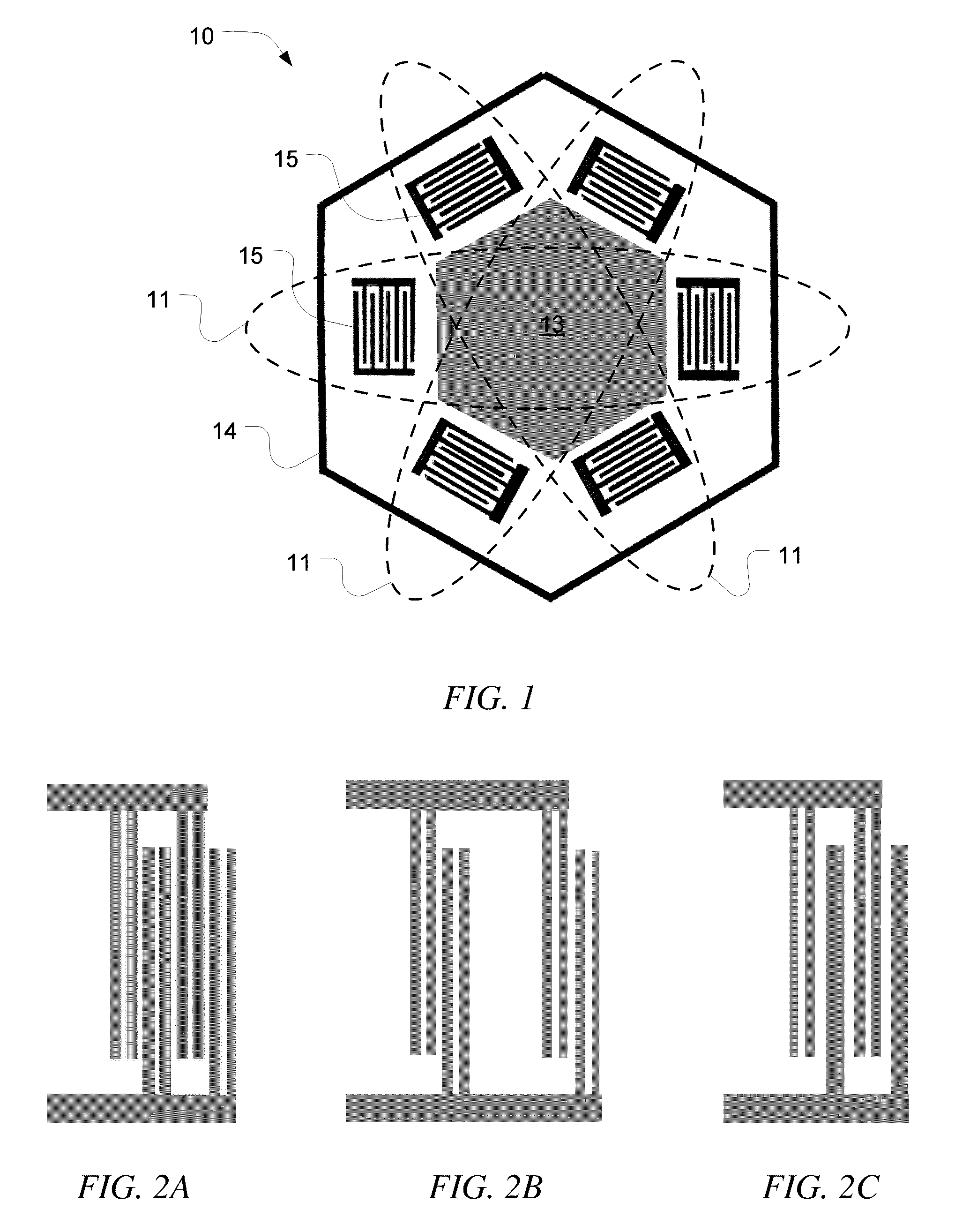
[0042]FIG. 1 provides a schematic of hexagonal SAW device 10. As shown, hexagonal SAW device 10 is a composite of three traditional delay lines 11 arranged about the center of the substrate die 14, which is approximately 20 mm×20 mm. The individual delay lines 11 are comprised of identical bi-directional IDTs 15 with an aperture of 47λ, delay length of 197λ, and feature size of 4 μm. The delay line is shorted to eliminate unwanted waves and eliminate the electrical effect. A standard metallization procedure of 100 nm titanium adhesion layer followed by 700 nm gold layer is used.
[0043]Sensitivity required for detection of many biological markers is on the order of a few nano-grams per milliliter, which is obtainable by many types of sensors; however, SAW sensors are some of the most sensitive and easy to implement devices. Challenges associated with this order of mass sensitivity become largely a fixture and test parameter issue because any variation in fluid flow or pressure will ca...
example 2
[0052]Hexagonal SAW device 10 is a composite of three traditional delay lines 11 arranged about the center of 36° YX LiTaO3 substrate die 14. The die 14 dimensions are approximately 20 mm×20 mm×0.5 mm. The individual delay lines 11 are comprised of identical bi-directional IDTs 15 with an aperture of 47λ and delay length of 197λ. Each IDT contains thirty finger pairs. The periodicity of the finger pairs is 40 microns and the aperture width is 200 microns. The transmitting and receiving IDTs are spaced 3.25λ apart. The delay line is shorted to eliminate unwanted waves and eliminate the electrical effect. A standard metallization procedure of 100 nm titanium adhesion layer followed by 700 nm gold layer is used.
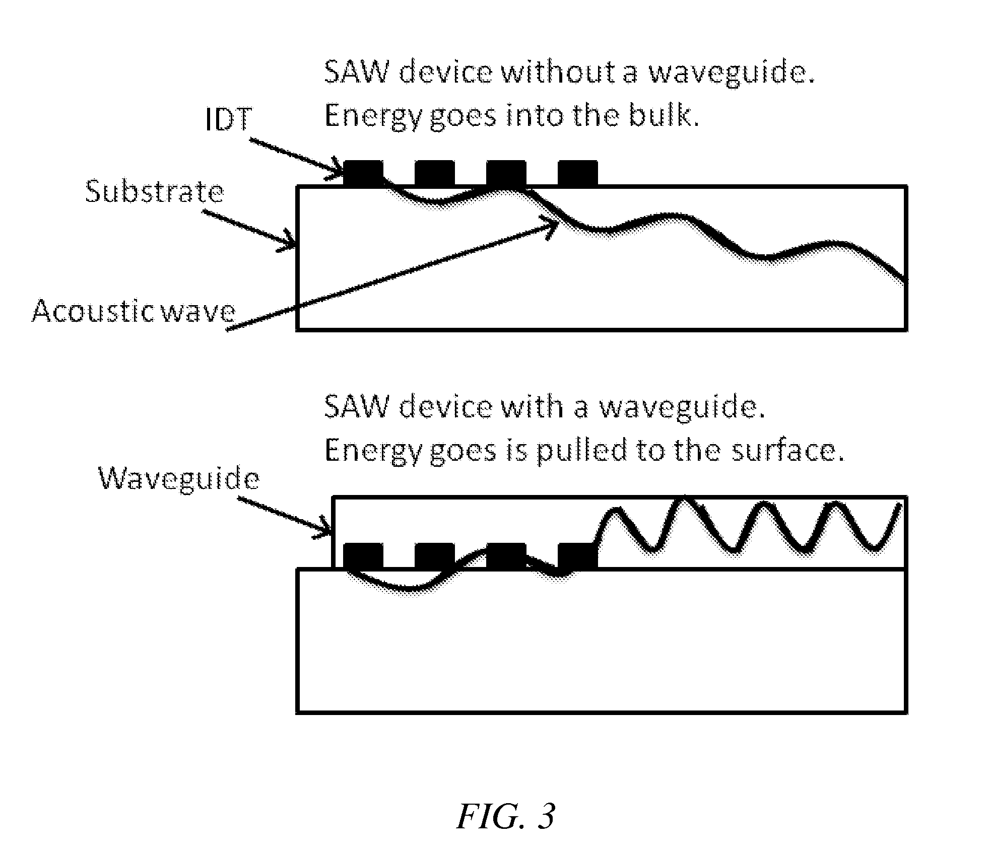
[0053]Upon fabrication of the IDTs on the lithium tantalite substrate, the waveguide is applied by spin coating the device with four weight-percent polystyrene in butoxyethyl acetate. The optimal thickness of the polystyrene is about 0.5 μm, which enables Love-wave generation. T...
PUM
| Property | Measurement | Unit |
|---|---|---|
| angle | aaaaa | aaaaa |
| aperture width | aaaaa | aaaaa |
| aperture width | aaaaa | aaaaa |
Abstract
Description
Claims
Application Information


