Transparent epoxy resin composition for molding optical semiconductor and optical semiconductor integrated circuit device using the same

a technology of optical semiconductor and epoxy resin, which is applied in the direction of semiconductor devices, solid-state devices, basic electric elements, etc., can solve the problems of filler or the like not being mixed in the resin, the package itself absorbs moisture, and the resin is difficult to re-mold. , to achieve the effect of excellent thermal discoloration resistance, excellent solder reflow resistance and excellent delamination

Active Publication Date: 2011-02-01
RENESAS ELECTRONICS CORP +1
View PDF12 Cites 1 Cited by
  • Summary
  • Abstract
  • Description
  • Claims
  • Application Information

AI Technical Summary

Benefits of technology

[0013]Accordingly, the present invention has been made to solve the above-mentioned problems in the related art. An object of the present invention is to provide a transparent epoxy resin composition for molding an optical semiconductor, that can suppress delamination between a semiconductor device and a molding resin, that exhibits excellent solder reflow resistance, and that has excellent thermal discoloration resistance even after a reflow step. Another object of the present invention is to provide an optical semiconductor integrated circuit device incorporating this transparent epoxy resin composition.
[0038]As a result of the study, they have found out that moisture vapor vaporizing in the solder reflow is released from the interface between the lead frame and the molding resin and that the problems caused in the solder reflow are effectively solved by improving the thermal discoloration resistance after the reflow step.
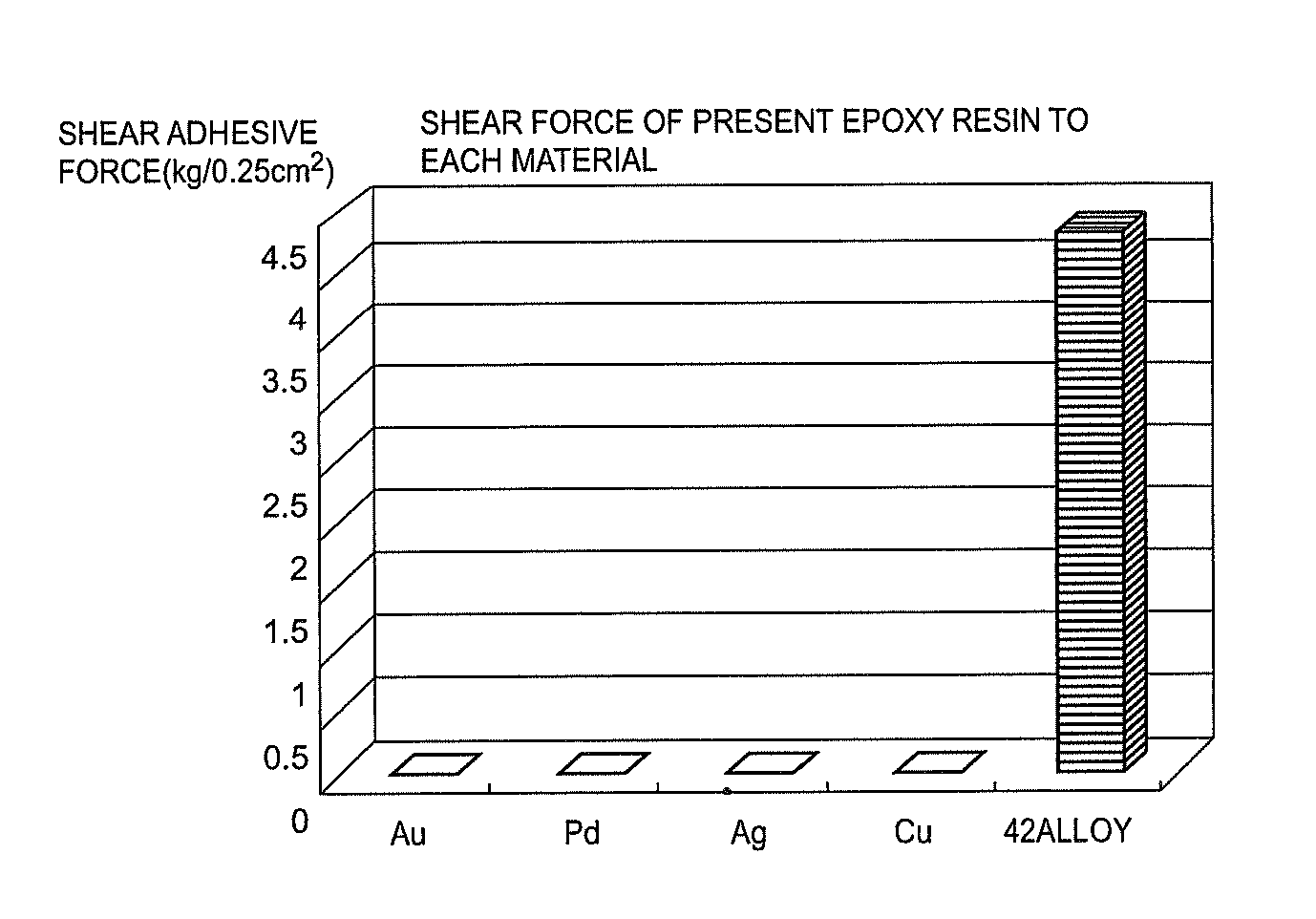
[0040]As a result, they have found that when a thiol, i.e., component (C), and an amine-based compound of a curing catalyst that is the above-mentioned component (D) are used together for the transparent epoxy resin composition that is a material for forming a molding resin (cured material), the adhesive force of the molding resin (cured material) to the lead frame is lowered and it is effective in thermal discoloration resistance. Therefore, they have achieved the present invention.
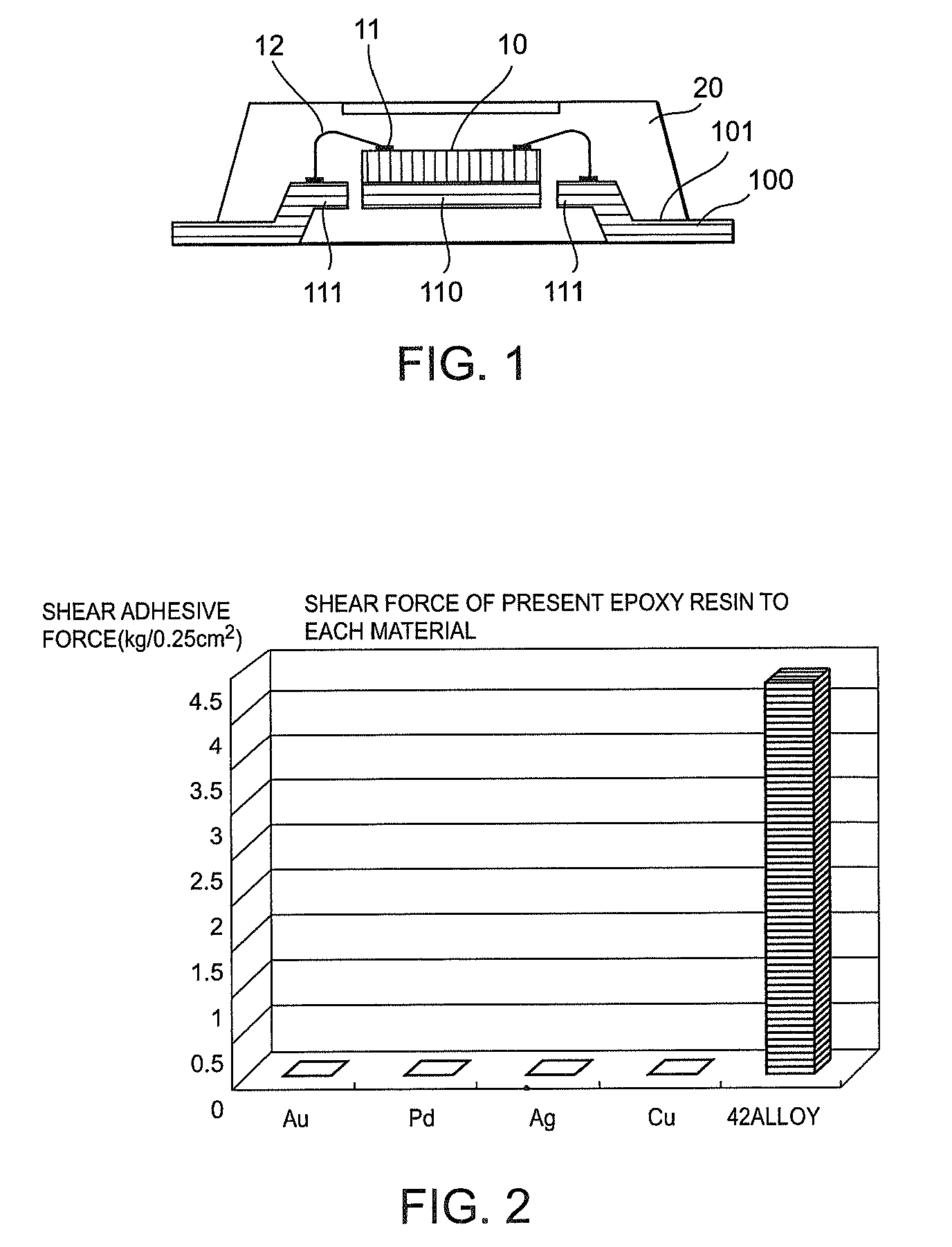
[0041]In particular, they have found out that water discharge property in the optical semiconductor device is enhanced by the lowering of the adhesive force of the molding resin (cured material) to the lead frame that a coating layer of silver or of palladium and gold is formed on an outermost layer of, which is frequently used as a lead frame in recent years, and thereby it is possible to provide excellent solder reflow resistance and excellent thermal discoloration resistance that are impossible to be obtained in a conventional transparent molding material. They have confirmed that even if optical semiconductor elements are highly integrated and the optical semiconductor device is enlarged in size, the water discharge in the device can be effectively performed.
[0042]Furthermore, they have found that when a specific silane coupling material is used as the above constituent of the transparent epoxy resin composition, the adhesive force of the molding resin to the optical semiconductor element is more improved, and this is more effective for the delamination and so forth in the solder reflow. This is effective particularly in the optical semiconductor integrated circuit in which the optical semiconductor elements in themselves are enlarged in size.
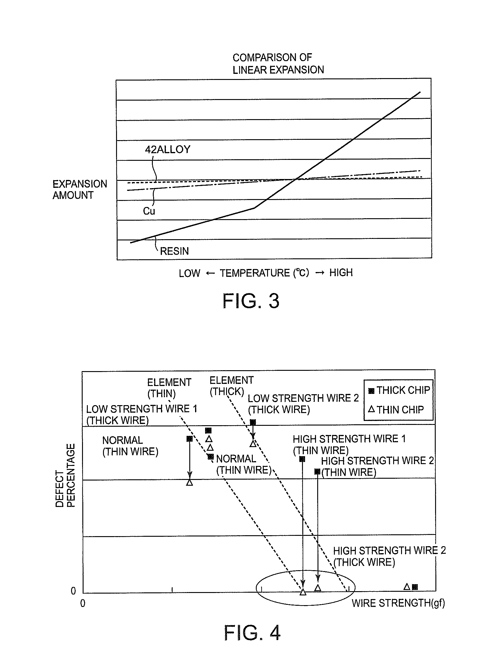
[0043]Moreover, when a glass transition point of this transparent epoxy resin composition is set to 90° C. to 120° C., change of phase is initiated as the resin cured material in this temperature range or higher so that the resin composition comes to have low elasticity. They have confirmed that heat stress in a high temperature can be reduced by utilizing the property of this low elasticity.

Problems solved by technology

Moreover, in recent years, regulation on lead has become more stringent due to environmental reasons, and this rendered it necessary to use high temperature as the reflow temperature.
Furthermore, when a known epoxy resin composition is used in the reflow step, the package itself absorbs moisture before being exposed to a high temperature.
Therefore, the absorbed moisture vaporizes to form moisture vapor during the solder reflow, and the moisture vapor pressure disadvantageously causes the optical semiconductor element to delaminate from the molding resin (cured member).
However, in an optical semiconductor device that emits / receives light, a filler or the like cannot be mixed in the resin because of its special characteristics.
In particular, unlike in other individual optical semiconductors such as LEDs, in an optical integrated circuit including enlarged optical semiconductor elements, it has become difficult to solve the problem due to the increased size of the optical semiconductor device itself.
However, this structure cannot completely resolve the problems of the optical integrated circuit device including a lead frame, namely, the problems of delamination during high-temperature solder reflow (260° C.) and discoloration in the molding resin.
However, when an optical semiconductor device including a lead frame is subjected to a high-temperature solder reflow (260° C.) by using this transparent epoxy resin composition, delamination, resin clacking, and discoloration of resin still occur.
Thus, it has not been possible to solve the problems.

Method used


Image

  • Transparent epoxy resin composition for molding optical semiconductor and optical semiconductor integrated circuit device using the same
  • Transparent epoxy resin composition for molding optical semiconductor and optical semiconductor integrated circuit device using the same
  • Transparent epoxy resin composition for molding optical semiconductor and optical semiconductor integrated circuit device using the same

Examples


Embodiment Construction

[0053]Next, embodiments of the present invention will be explained in detail.

[0054]The transparent epoxy resin composition for molding an optical semiconductor of the present invention can be obtained by using an epoxy resin (component (A)), a curing agent (component (B)), a thiol-containing compound (a component (C)), and an amine-based curing catalyst represented by the following formula as the curing catalyst:

[0055]

[0056]R1 is a hydrogen atom (—H), an alkyl group, or a phenyl group.

[0057]R2 is an alkyl group (—CH3, —C2H5, —C3H7).

In general, the transparent epoxy resin composition is in the form of liquid, powder, or tablets made from the powder.

[0058]The epoxy resin (component (A)) usable in the present invention is not particularly limited and may be any common transparent epoxy resin.

[0059]Examples of the transparent epoxy resins include bisphenol A type epoxy resin, a bisphenol F type epoxy resin, a phenol novolac type epoxy resin, a cresol novolac type epoxy resin, an alicycl...


PUM

PropertyMeasurementUnit
glass transition pointaaaaaaaaaa
heat resistanceaaaaaaaaaa
temperatureaaaaaaaaaa

Abstract

In an optical semiconductor integrated circuit device using a lead frame, a transparent epoxy resin composition for molding an optical semiconductor contains (A) an epoxy resin; (B) a curing agent; (C) a thiol; and (D) an amine-based curing catalyst represented by following Chemical Formula 1:R1: a hydrogen atom (—H), an alkyl group, or a phenyl groupR2: an alkyl group (—CH3, —C2H5, —C3H7).

Description

[0001]This application claims priority to prior Japanese patent application JP 2006-020431, the disclosure of which is incorporated herein by reference.BACKGROUND OF THE INVENTION[0002]1. Field of the Invention[0003]The present invention relates to a structure of a resin-molded or resin-sealed optical semiconductor integrated circuit device including a lead frame and a transparent resin, in particular, to a structure of an optical semiconductor integrated circuit device having excellent thermal discoloration resistance and crack resistance against high-temperature reflow in the implementation of mounting the optical semiconductor integrated circuit device to equipment.[0004]2. Description of the Related Art[0005]A transparent epoxy resin composition is generally used for resin-molding or resin-sealing an optical semiconductor element such as a light-sensitive element and a light-emitting element mounted in a compact disk (CD) player, a digital versatile disk (DVD) player, or the lik...

Claims


Application Information

Patent Timeline
Patent Type & Authority Patents(United States)
IPC IPC(8): H01L23/495H01L33/54H01L33/56H01L33/62
CPCC08G59/4215C08G59/66C08G59/686H01L2224/45144H01L2224/48091H01L2224/48247H01L2224/48471H01L24/45H01L2924/00014H01L2924/14H01L2924/181H01L2924/1815H01L2924/00H01L2924/00012H01L2224/4554C08L63/00C08K5/17
Inventor UCHIDA, KENJIHIRASAWA, KOKISHIMADA, KATSUMIUENISHI, SHINJIROOTA, SHINYA
Owner RENESAS ELECTRONICS CORP
Why Eureka
Try Eureka