Optical lithography correction process

a technology of optical lithography and correction process, applied in the field of optical lithography correction process, can solve the problems of increasing manufacturing costs, unable to provide any help in actual production, and unable to meet the requirements of the final microcircui

Inactive Publication Date: 2011-02-01
CADENCE DESIGN SYST INC
View PDF10 Cites 150 Cited by
  • Summary
  • Abstract
  • Description
  • Claims
  • Application Information

AI Technical Summary

Problems solved by technology

Concomitantly, the impact of erroneous corrections has also increased leading to circuit failures and, therefore, delays in the delivery of the final microcircuit.
Unfortunately, these techniques do not provide any help in actually resolving the issues raised and, thus, still cause delays and increase manufacturing costs.

Method used


Image

  • Optical lithography correction process
  • Optical lithography correction process
  • Optical lithography correction process

Examples


Embodiment Construction

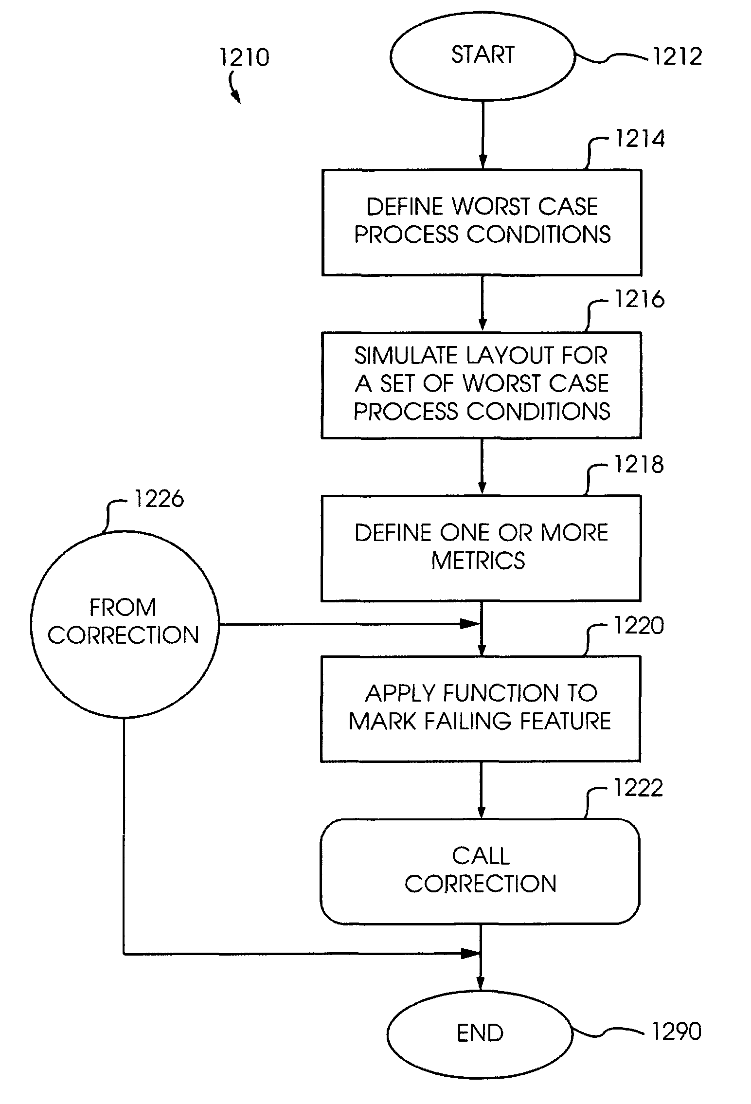
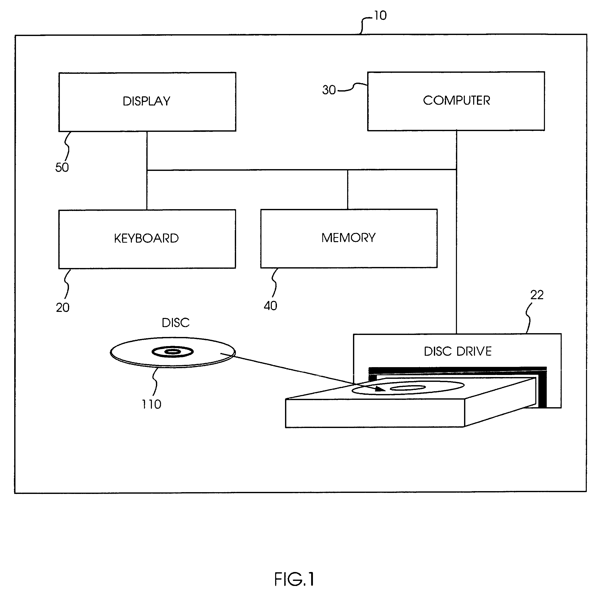
[0020]Referring now to the drawings and more particularly to FIGS. 1 and 12, there is illustrated a computer-aided design (CAD) system 10, which is constructed according to one of the preferred embodiments of the present invention. In this embodiment, the CAD system 10, through a computer readable program product 110, implements a resolution enhancement technique 1210 (FIG. 12) in an optical lithography process. More particularly, through an optical rule checking (ORC) process, the resolution enhancement technique 1210 verifies whether a distorted mask solution in fact creates the necessary effects to significantly reduce the risk of pattern failures in the printing process, and effectively increase the throughput of a nano-circuit production run when utilizing silicon wafer features having size dimensions significantly smaller than the wavelength of light. In this regard, the resolution enhancement technique 1210 characterizes the influence of individual ones of a plurality of wors...


PUM


Abstract

A apparatus and method for correcting a process critical layout includes characterizing the influence of individual ones of a set of worst case process variations on a simulated nano-circuit layout design and then correcting layout geometries in the simulated nano-circuit layout based on such characterizations.

Description

BACKGROUND OF THE INVENTIONBackground of Prior Art[0001]As optical lithography attempts to print smaller and smaller features relative to the wavelength of light used for imaging, the extent to which optical proximity correction techniques modify the original layout has dramatically increased. Concomitantly, the impact of erroneous corrections has also increased leading to circuit failures and, therefore, delays in the delivery of the final microcircuit. Therefore, there is a strong desire to check the validity of the optical proximity corrections before committing a corrected layout to the mask manufacturing process. This need has resulted in the creation of optical rule checking (ORC) techniques. These techniques validate the final result of the optical proximity correction by comparing the predicted images to the original layout. This process has greatly helped minimize delays in the nano-circuit fabrication as potentially fatal errors are detected much earlier then was previousl...

Claims


Application Information

Patent Timeline
Patent Type & Authority Patents(United States)
IPC IPC(8): G06F17/50G06F9/45
CPCG03F1/144G03F1/36G03F7/70441G06F2217/12Y10S977/834G06F2119/18Y02P90/02
Inventor ZACH, FRANZ XAVER
Owner CADENCE DESIGN SYST INC
Why Eureka
Try Eureka