Constraint assistant for circuit design

a technology of constraint assistant and circuit design, applied in the direction of computing, instruments, electric digital data processing, etc., can solve the problems of limited ability of a given ic fabrication process to maintain tolerances for electrical characteristics of components, reduce focus and alignment problems, and inability to measure each device on an individual basis. , to achieve the effect of avoiding time-consuming and error-prone manual determination, less likely to make costly mistakes, and enhancing sub-circuit determination

Inactive Publication Date: 2008-08-26
CADENCE DESIGN SYST INC
View PDF4 Cites 114 Cited by
  • Summary
  • Abstract
  • Description
  • Claims
  • Application Information

AI Technical Summary

Benefits of technology

[0010]Additionally, the present invention can be implemented in another embodiment to provide an improved user interface for displaying such subcircuit networks with simultaneous highlighting of corresponding circuit components and connections in corresponding circuit schematic and layout displays. This assists a designer in deciding whether or not a recognized subcircuit is appropriate for the application of recommended layout constraints. This is also useful for checking circuit schematics for connectivity errors. The user interface can be designed to provide expert physical circuit layout assistance to a designer in a conveniently formatted display showing the type of subcircuit detected and recommended layout constraints for consideration and selection. A less experienced designer may learn the “art” of physical circuit layout from this feature, and is far less likely to make costly mistakes that a more experience designer might avoid. An expert circuit designer avoids the time-consuming and error-prone manual selection of schematic elements and application of layout constraints for use during the generation of corresponding physical layouts. The circuit designer can also check his work for accuracy and completeness.
[0011]In an embodiment of the invention, subcircuits are determined through the correlation of potential subcircuit netlists with netlist types corresponding to known subcircuit types in a subcircuit-type library. In a further embodiment of the invention, subcircuit determination is enhanced through the examination of the positional placements and orientations of symbols representing subcircuit components in a circuit schematic drawing, i.e. “schematic format examination” (“SFE”). SFE makes use of circuit schematic drawing symmetry, and other drawing conventions for schematic depictions of subcircuits, to speed the selection of subcircuit netlists for correlation with netlist types by identifying likely subcircuit components. The schematic drawing conventions that are used to identify likely subcircuit components are mostly familiar to circuit designers from textbook, engineering class, and workplace exposure. Knowledge of recognized format conventions also allows a circuit designer to encourage or discourage the automatic identification of a potential subcircuit by adjusting the schematic drawing format, without changing circuit connectivity. The various embodiments of the present invention are referred to herein as a layout constraint assistant tool.

Problems solved by technology

Also, exposing a large surface area wafer sequentially in repeated fields reduces focus and alignment problems associated with the wafer's surface not being perfectly planar.
The capabilities of a given IC fabrication process to maintain tolerances for electrical characteristics of components are limited.
This limitation results because all IC components are fabricated and interconnected simultaneously.
No practical capability exists for measuring each device on an individual basis and then accepting or rejecting that device for use in a particular circuit, as is the case for circuits assembled of discrete components and PCBs.
But this matching of IC components is not perfect.
Spatially non-uniform processing conditions during wafer fabrication often result in component characteristic variations within a given IC.

Method used


Image

  • Constraint assistant for circuit design
  • Constraint assistant for circuit design
  • Constraint assistant for circuit design

Examples


Embodiment Construction

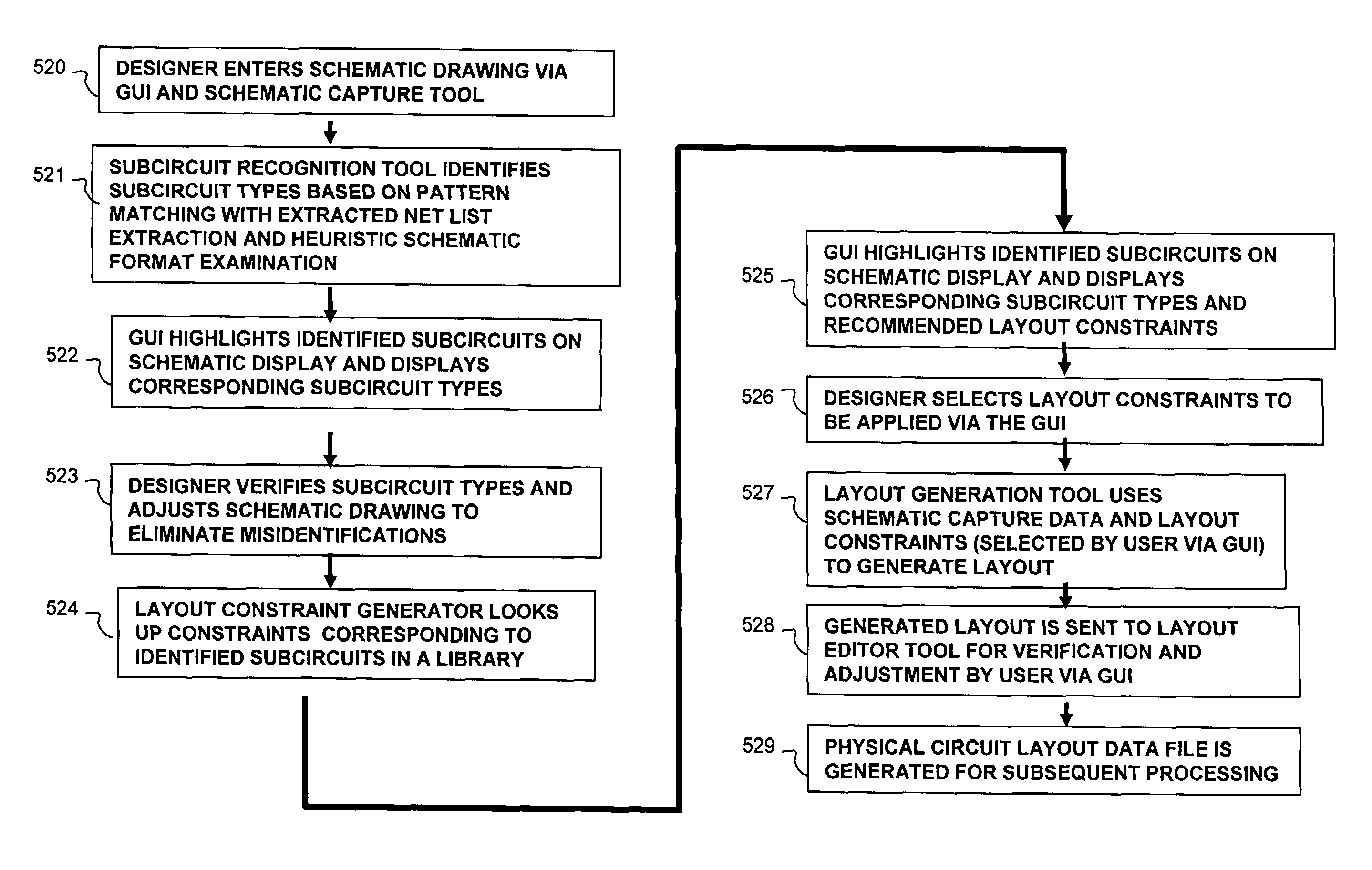
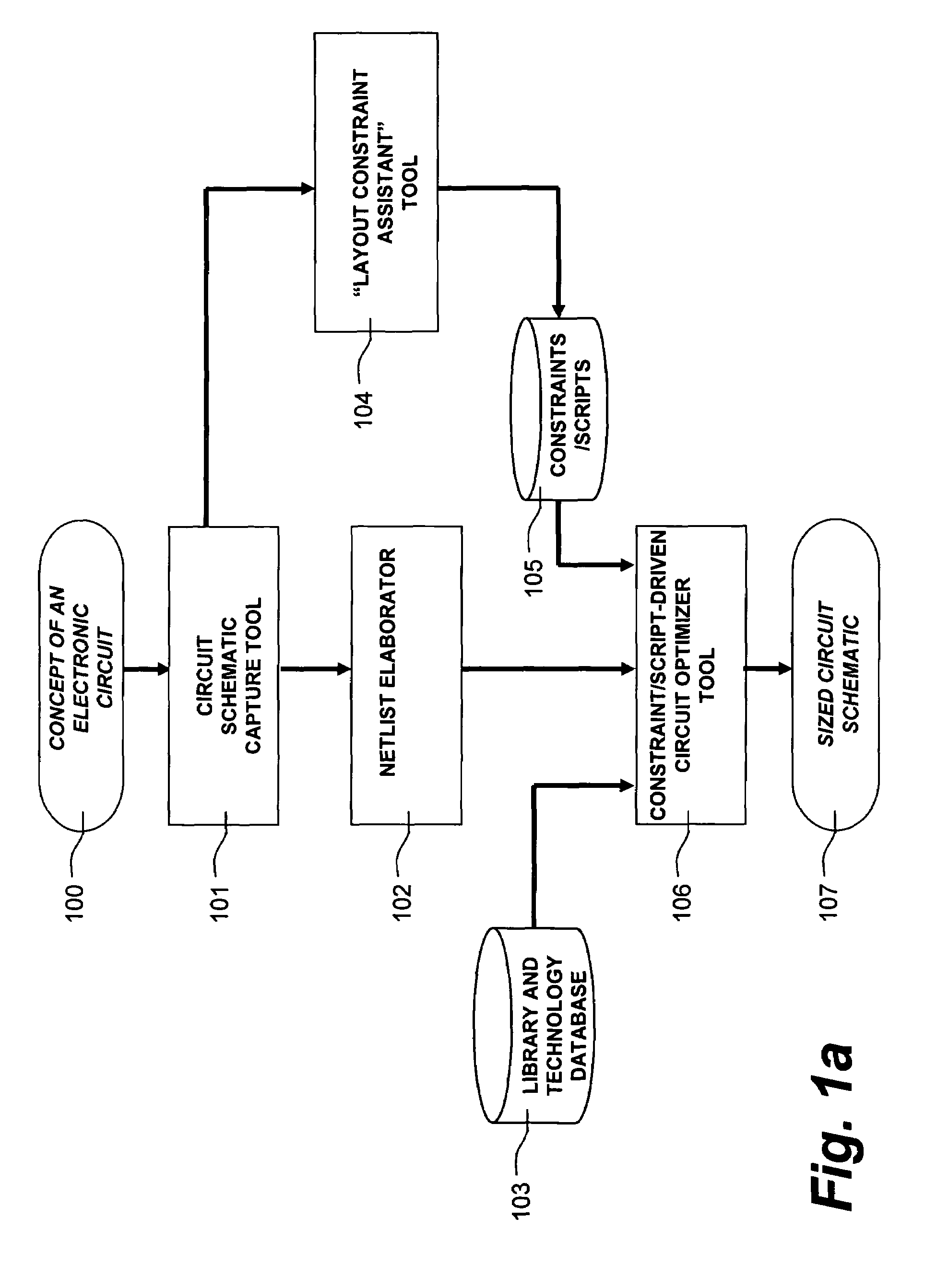
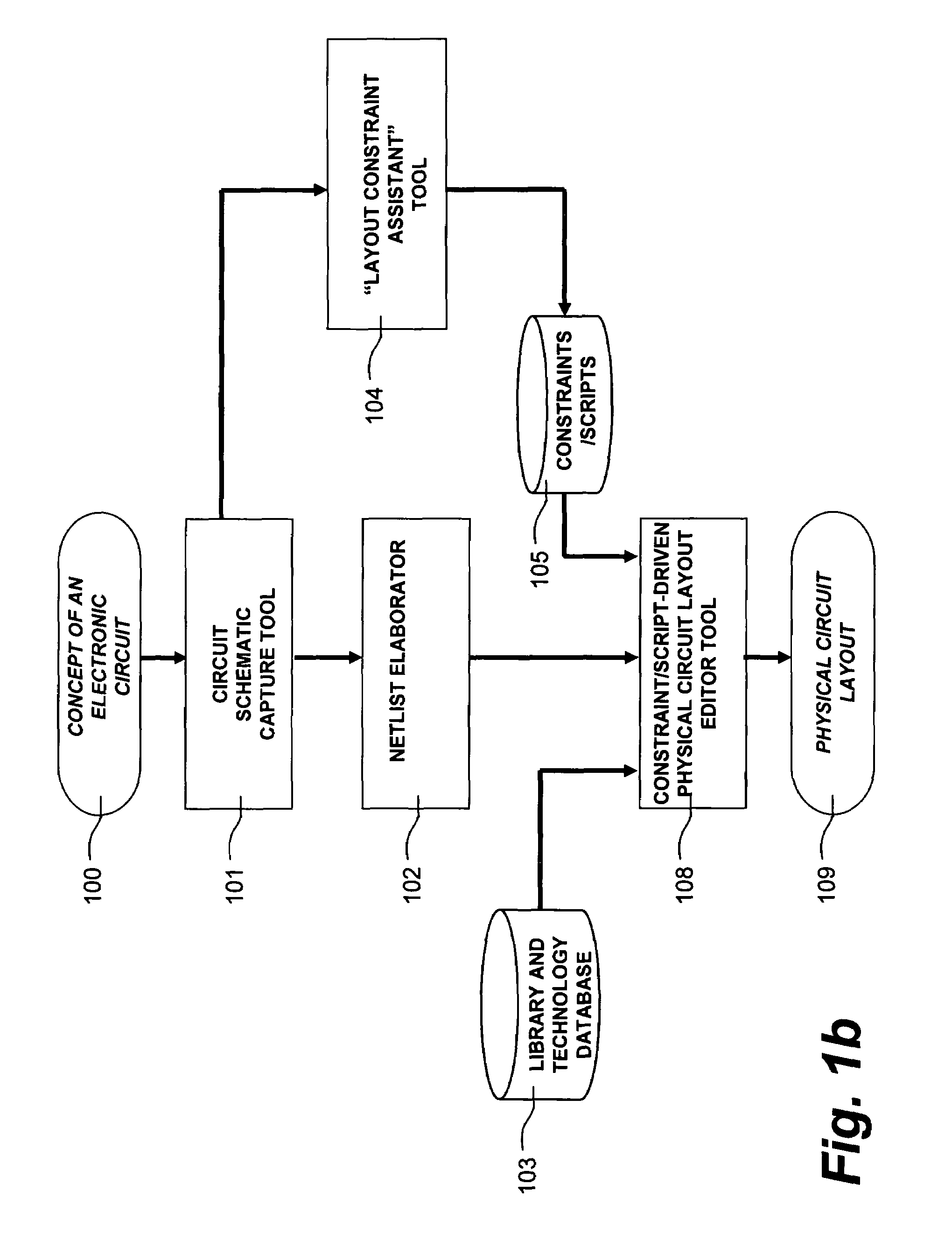
[0026]The present invention is directed toward a system and method of creating physical circuit layouts and parameter relationship constraints for different components in a subcircuit for circuit optimization using circuit simulations. According to one aspect of the invention, layout constraints for physical circuit layouts or parameter relationship constraints are assigned on the basis of subcircuit type as automatically determined by the examination of a circuit schematic, as well as other information.

[0027]Parameter relationship constraints will also be referred to herein as “logical constraints.” When a designer wants to size his circuit, he needs to care about logical constraints. For example, a current mirror is made of at least two transistors. In case of a current mirror made of MOSFETs, all transistors must have the same gate length for matching reasons.

[0028]Therefore, gate length matching is a logical constraint. For the same current mirror, the current ratio is roughly g...


PUM


Abstract

A computer aided design tool and method for designing IC layouts by recommending subcircuit layout constraints based upon an automated identification from a circuit schematic of subcircuit types requiring special IC layout constraints. Subcircuit types are identified on the basis of netlist examination, as well as cues from the layout of the circuit schematic.

Description

BACKGROUND OF THE INVENTION[0001]1. Field of the Invention[0002]The present invention relates to computer-aided design and design analysis tools for electronic integrated circuits, specifically computer aided design tools and methods for providing a circuit designer with improved means for designing physical circuit layouts.[0003]2. Description of the Related Art[0004]Electronic circuits form the building blocks of electronic devices. Electronic integrated circuits (“ICs”) based on silicon, or other semiconductor, technologies have revolutionized many aspects of everyday life because of high functionality, compact size, low power consumption, and low cost. Whereas conventional electronic circuits usually embody from a few to hundreds of electronic components, including ICs, a single IC can embody from a few to many millions of electronic components such as transistors, diodes, resistors, capacitors, and many others, along with associated interconnections. The various components for ...

Claims


Application Information

Patent Timeline
Patent Type & Authority Patents(United States)
IPC IPC(8): G06F17/50
CPCG06F17/5081G06F2217/74G06F30/398G06F2111/12
Inventor SONNARD, JEAN-DANIELWANG, ZHIGANGSAMPATH, HEMANTH
Owner CADENCE DESIGN SYST INC
Why Eureka
Try Eureka