

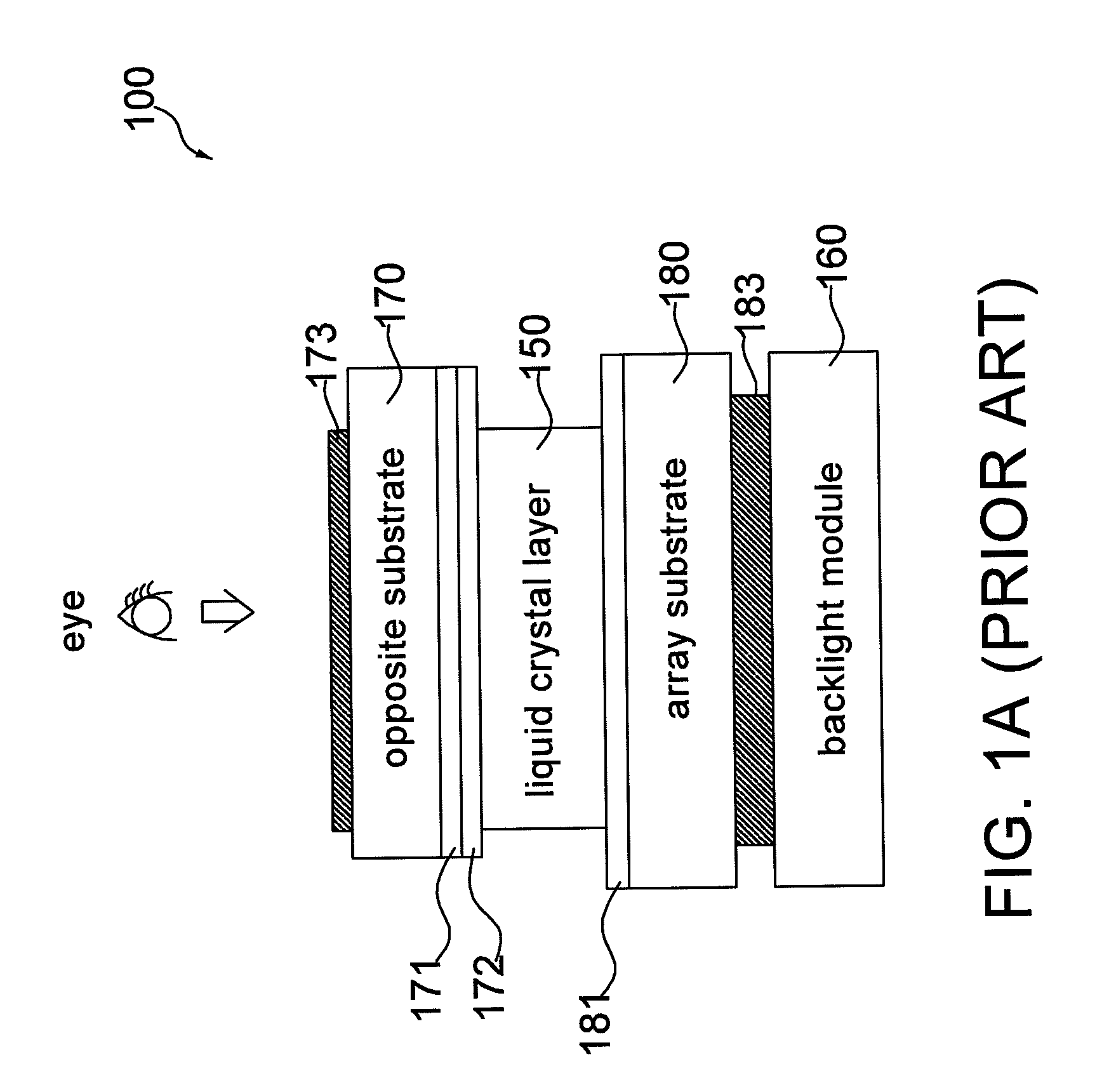
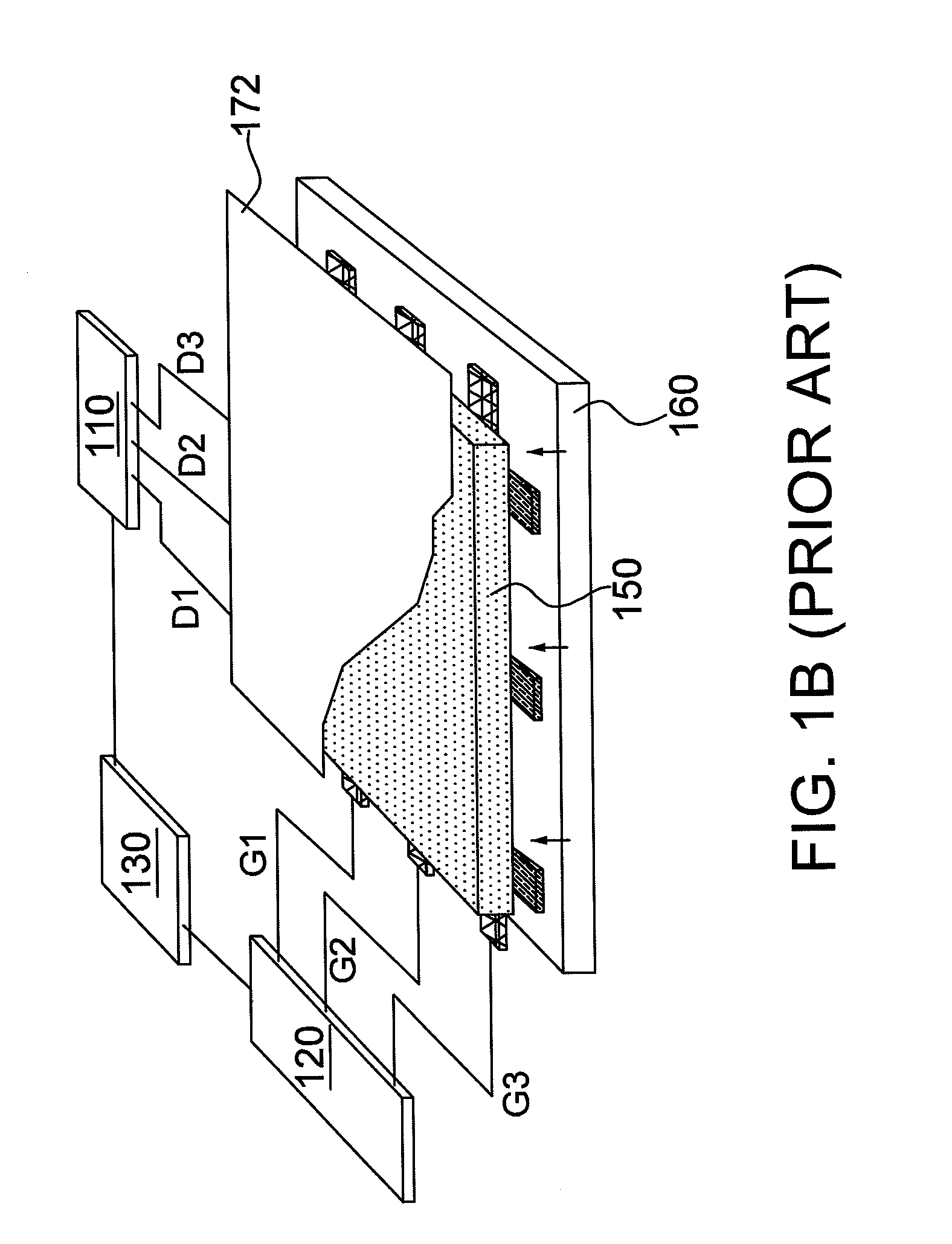
Touch display device
a display device and touch technology, applied in the field of touch display devices, can solve the problems of reducing the luminance of the display device and increasing the cost of hardwar
- Summary
- Abstract
- Description
- Claims
- Application Information
AI Technical Summary
Problems solved by technology
Method used
Image

Examples
first embodiment
[0071]FIG. 7A is a circuit schematic diagram of a sensing circuit according to the invention. Referring to FIG. 7A, a sensing circuit 710 includes a driving unit 610 and a detecting unit 620A. The driving unit 610 includes a wave generator 711 and a voltage driver 712 while the detecting unit 620A includes a buffer 713 and a signal extracting unit 714.
[0072]Referring to FIGS. 6A and 7A, according to a fixed frequency f1, the wave generator 711 generates a digital signal m having a fixed period T(=1 / f1) within each measurement time interval tm. According to the digital signal m, the voltage driver 712 sequentially supplies an analog signal a to all the gate signals G1-Gn through a transistor Rz and the multiplexer 630, thereby to perform fixed-period signal measurement. Because of the properties of a high input impedance and a low output impedance, the buffer 713 is configured to isolate the scan lines G1-Gn from the signal extracting unit 714. The input impedance of the buffer 713 i...
fifth embodiment
[0082]FIG. 9A is a simplified diagram showing FIG. 7E in which no finger is placed on the touch display device of the invention. Referring to FIG. 9A, when no finger is placed on the touch display device, the output voltage Vin1 of the differential amplifier 742 has the same period as the square waves a and ā, representing the square waves a and ā and the output voltage Vin1 have the same sequences.
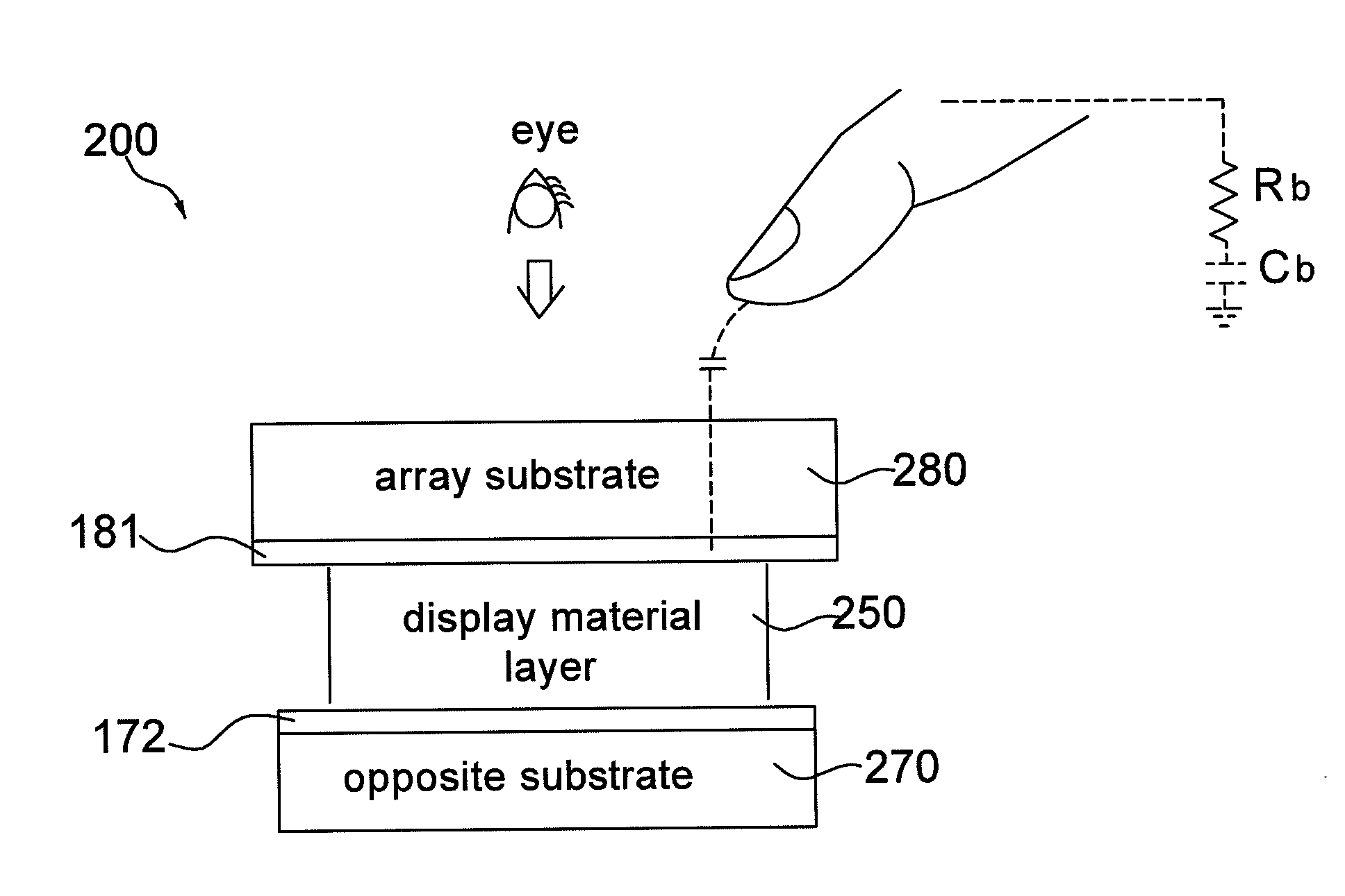
[0083]FIG. 9B is a simplified diagram showing the fifth embodiment of FIG. 7E in which a finger touch is simultaneously detected by two scan lines connected with two input terminals of the same differential amplifier. Referring to FIG. 9B, when a finger is placed on the touch display device of the invention and a finger touch is simultaneously detected by two scan lines connected with two input terminals of the same differential amplifier, a current leakage path from the two scan lines through the human body to ground is created. As a result of voltage division, the amplitudes of two inpu...
eighth embodiment
[0088]FIG. 7H is a circuit schematic diagram of a sensing circuit according to the invention. Comparing FIGS. 7D and 7H, a sensing circuit 780 is similar to the sensing circuit 740. A difference between them is that the sensing circuit 780 has a differential structure. A detecting unit 620H includes a differential amplifier 742, an ADC 715 and a RMS unit 732. Here, when the RMS unit 732 is a digital circuit, the RMS unit 732 operates with the ADC 715. However, when the RMS unit 732 is an analog circuit, the RMS unit 732 operates without the ADC 715. The ADC 715 is an optional element and thus represented in dotted lines.
[0089]It is noted that, although either the driving signal a or the two complementary driving signals a and ā shown in FIGS. 7A-7H are square waves, they can be implemented using sinusoidal waves, or triangular waves, or any other periodic waves.
[0090]FIG. 6C is a simplified diagram showing the embodiment of FIG. 6A in which three scan lines form a sensing channel. N...
PUM
 Abstract
Description
Claims
Application Information