Pseudo-differential interfacing device having a switching circuit

a technology of switching circuit and interfacing device, which is applied in the direction of logic circuit coupling/interface arrangement, digital transmission, pulse technique, etc., can solve the problems of affecting the performance of nearby circuits, and causing unwanted couplings

Inactive Publication Date: 2011-02-08
ZXNOISE LLC
View PDF15 Cites 230 Cited by
  • Summary
  • Abstract
  • Description
  • Claims
  • Application Information

AI Technical Summary

Benefits of technology

[0025]It is an object of the interfacing device of the invention to provide pseudo-differential transmission through an interconnection having two or more transmission conductors, the transmission presenting reduced unwanted couplings.
[0042]According to the invention, the common terminal switching circuit in the closed state may be such that, at said first quiescent operating point, said first passive two-terminal circuit element has a small-signal impedance having, in said known frequency band, an absolute value less than or equal to three hundred ohms. The set of the dynamic impedances defined by this inequality is such that, when said transmitting circuit is in the activated state, the currents injected in the transmission conductors may be associated with return currents flowing mainly in the common conductor of said interconnection, which must be connected to said common terminal. The specialist understands that this situation allows reduced unwanted couplings with other electronic circuits near the interconnection.
[0072]A device of the invention may be such that it constitutes a part of an integrated circuit, each of said m signal terminals being coupled to one or more pins of said integrated circuit, said common terminal being coupled to one or more pins of said integrated circuit. This configuration is appropriate when said interconnection is realized outside said integrated circuit. The specialist notes that if there are many signal terminals, for instance more than 16 signal terminals, the absolute value of the current which may flow through the common terminal may become much larger than the maximum absolute value of the current flowing through a single signal terminal. Consequently, in this case, if a single pin is allocated to the common terminal, a degradation of transmission may occur for fast signals, because of the inductance of a connection using a single pin. In this case, using several pins for the common terminal reduces this inductance and improves transmission.

Problems solved by technology

This scheme is vulnerable to the noise produced by some electromagnetic couplings between some conductors of said interconnection and other nearby conductors, for instance when said interconnection and these other conductors are built on the same printed circuit board.
The specialist understands that this situation often creates unwanted couplings with other electronic circuits near the interconnection.
Consequently, these terminations increase the generation of electromagnetic disturbances which may degrade the performances of nearby circuits, and the vulnerability to electromagnetic disturbances produced by nearby circuits.
However, prior art transmitting circuits for pseudo-differential transmission nevertheless produce return currents flowing mainly in the reference conductor or in a power supply conductor.
Consequently, because of the limitations of these prior art transmitting circuits, prior art pseudo-differential systems for transmission generate electromagnetic disturbances which may degrade the performances of nearby circuits, and are vulnerable to electromagnetic disturbances produced by nearby circuits.

Method used


Image

  • Pseudo-differential interfacing device having a switching circuit
  • Pseudo-differential interfacing device having a switching circuit
  • Pseudo-differential interfacing device having a switching circuit

Examples


first embodiment (

Best Mode)

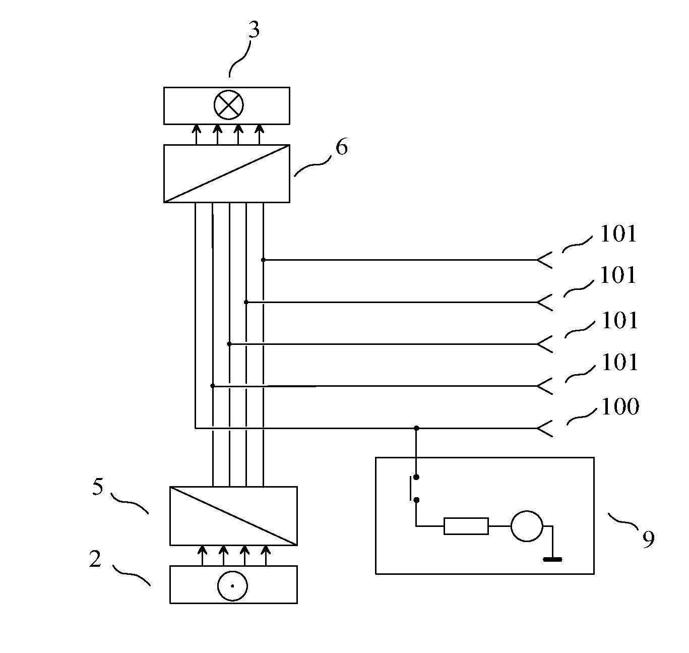
[0096]As a first embodiment of an interfacing device of the invention, given by way of non-limiting example and best mode of carrying out the invention, we have represented in FIG. 3 an interfacing device of the invention built inside an integrated circuit, comprising m=4 signal terminals (101) and a common terminal (100), the signal terminals (101) and the common terminal (100) being intended to be connected to an interconnection having at least m+1=5 conductors.

[0097]A transmitting circuit (5) receives q=4 “input signals of the transmitting circuit” coming from a source (2), the output of the transmitting circuit being coupled to the 4 signal terminals (101). The output of the transmitting circuit is not coupled to the common terminal (100). The output of the transmitting circuit (5) delivers, when the transmitting circuit is in the activated state, q=4 transmission variables, each transmission variable being a voltage between one of said signal terminals (101) and the r...

second embodiment

[0113]The second embodiment of an interfacing device of the invention, given by way of non-limiting example, comprises:[0114]the transmitting circuit and the common terminal switching circuit shown in FIG. 5;[0115]the receiving circuit and the termination circuit shown in FIG. 7.

[0116]In the transmitting circuit and the common terminal switching circuit shown in FIG. 5:[0117]each of the q=3 “input signals of the transmitting circuit” is applied to a signal input (57) which is of the single-ended input type;[0118]each of the q=3 signal inputs (57) corresponds to a three-transistor cell made of an input transistor (511) and of a current mirror comprising two transistors (512) (513);

[0119]each of the m=3 signal terminals (101) is coupled to the drain of the output transistor (513) of the corresponding three-transistor cell;[0120]the transmitting circuit is made of the three three-transistor cells, hence of 9 transistors (511) (512) (513);[0121]a “common terminal switching signal” is ap...

third embodiment

[0139]The third embodiment of an interfacing device of the invention, given by way of non-limiting example, comprises the common terminal switching circuit shown in FIG. 6, consisting of an n-channel transistor (912) and of a p-channel transistor (913) the sources of which are connected to each other and the drains of which are connected to each other. The drains of the transistors (912) (913) are connected to the common terminal (100) and the sources of the transistors (912) (913) are grounded. This common terminal switching circuit is controlled by two control inputs: a first control input (581) for the “first common terminal switching signal” and a second control input (582) for the “second common terminal switching signal”. The specialist sees that the two transistors (912) (913) form a CMOS switch and understands that the “source” and “drain” electrodes may be exchanged in FIG. 6, when the transistors are symmetrical.

[0140]When the “first common terminal switching signal” appli...


PUM


Abstract

The invention relates to an interfacing device for pseudo-differential transmission through interconnections used for sending a plurality of electrical signals. The interfacing device of the invention includes signal terminals and a common terminal. A transmitting circuit receives the input signals of the transmitting circuit coming from a source. The output of the transmitting circuit delivers, when the transmitting circuit is in the activated state, voltages between one of the signal terminals and the reference terminal (ground). A receiving circuit delivers, when the receiving circuit is in the activated state, output signals of the receiving circuit determined each by the voltage between one of the signal terminals and the common terminal, to the destination. In the closed state, the common terminal switching circuit is, for the common terminal, equivalent to a voltage source delivering a constant voltage, connected in series with a passive two-terminal circuit element presenting a low impedance.

Description

CROSS-REFERENCE TO RELATED APPLICATIONS[0001]The present application claims the benefit of priority to International Patent Application No. PCT / IB2008 / 051982 filed 20 May 2008, which further claims the benefit of priority to France Patent Application No. 0704949 filed 09 Jul. 2007, the contents of which are incorporated herein by reference in their entirety.FIELD OF THE INVENTION[0002]The invention relates to an interfacing device for pseudo-differential transmission through interconnections used for sending a plurality of electrical signals, such as the interconnections made with multiconductor cables, or with the traces of a printed circuit board, or inside an integrated circuit.[0003]The French patent application Ser. No. 07 / 04949 of 9 Jul. 2007, entitled “Dispositif d'interface pseudo-différentiel avec circuit de commutation” is incorporated by reference.PRIOR ART[0004]Let us consider the problem of transmission through an interconnection, for obtaining m transmission channels, ...

Claims


Application Information

Patent Timeline
Patent Type & Authority Patents(United States)
IPC IPC(8): H03K19/0175
CPCH04L25/0276H04L25/085
Inventor BROYDE, FREDERICCLAVELIER, EVELYNE
Owner ZXNOISE LLC
Why Eureka
Try Eureka