Method of pattern transfer
a pattern and circuit technology, applied in the field of pattern transfer, can solve the problem that the pattern cannot be corrected, and achieve the effect of improving the resolution of the first pattern transfer, reducing the deviation caused by the optical proximity effect, and high resolution
- Summary
- Abstract
- Description
- Claims
- Application Information
AI Technical Summary
Benefits of technology
Problems solved by technology
Method used
Image
Examples
fourth embodiment
[0037]FIG. 27 to FIG. 34 are schematic views of a fabricating process in the present invention. In this embodiment, the circuit pattern 100 should be transferred to the substrate 150 (shown in FIG. 30) on the wafer 150. The circuit pattern 100 comprises a dense pattern region 102 and an iso pattern region 104. The dense pattern region 102 comprises a plurality of dense patterns 106 positioned densely and the iso pattern region 104 comprises at least an iso pattern 108 with large pitch. In this embodiment, the width W1 of the dense patterns 106 and of the iso pattern 108 is very small, e.g. 60 to 80 nm, which already exceeds the size limit for fabrication in traditional lithography technology.
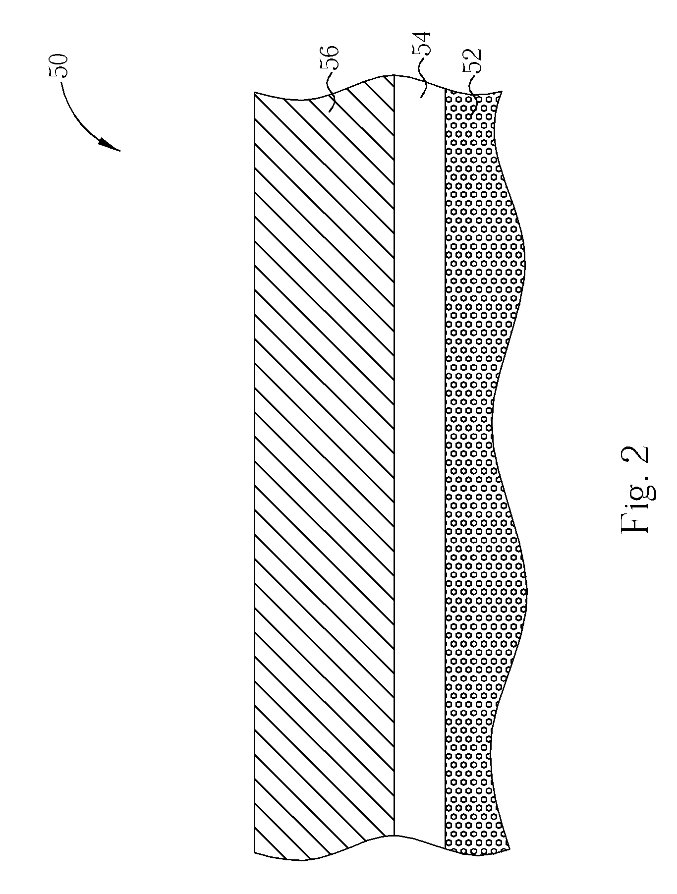
[0038]A hard mask layer 154 and a first photoresist layer 156 (shown in FIG. 30) are formed sequentially on the surface of the substrate 152 before the pattern transfer. As shown in FIG. 28, a first lithography pattern 110 comprises a plurality of the lithography circuit patterns 112, indicated ...
fifth embodiment
[0041]FIG. 35 to FIG. 37 are schematic views of a fabricating process in the present invention. In this embodiment, the circuit pattern 200 should be transferred to a wafer. The circuit pattern 200 comprises a plurality of patterns having random pitch, e.g. patterns of the contact holes 202, dual patterns of the contact holes 204, triple patterns of the contact holes 206, or linear patterns. In order to increase the process window of the patterns having different pitch and shape, based on the principle of the present invention, a hard mask layer and a first photoresist layer are formed on the wafer. Then, a first lithography pattern 210 is provided, which comprises the patterns corresponding to the circuit pattern 200 (indicated by a dotted pattern), e.g. lithography patterns of the contact holes 212, dual lithography patterns of the contact holes 214, and triple lithography patterns of the contact holes 216 corresponding to patterns of the contact holes 202, dual patterns of the co...
PUM
| Property | Measurement | Unit |
|---|---|---|
| wavelength | aaaaa | aaaaa |
| width W1 | aaaaa | aaaaa |
| width W2 | aaaaa | aaaaa |
Abstract
Description
Claims
Application Information


