

Semiconductor device and method of manufacturing the same
a technology of semiconductor devices and semiconductors, applied in the field of semiconductor devices, can solve problems such as the complicated manufacturing process of semiconductor devices
- Summary
- Abstract
- Description
- Claims
- Application Information
AI Technical Summary
Benefits of technology
Problems solved by technology
Method used
Image

Examples
first embodiment
A First Embodiment
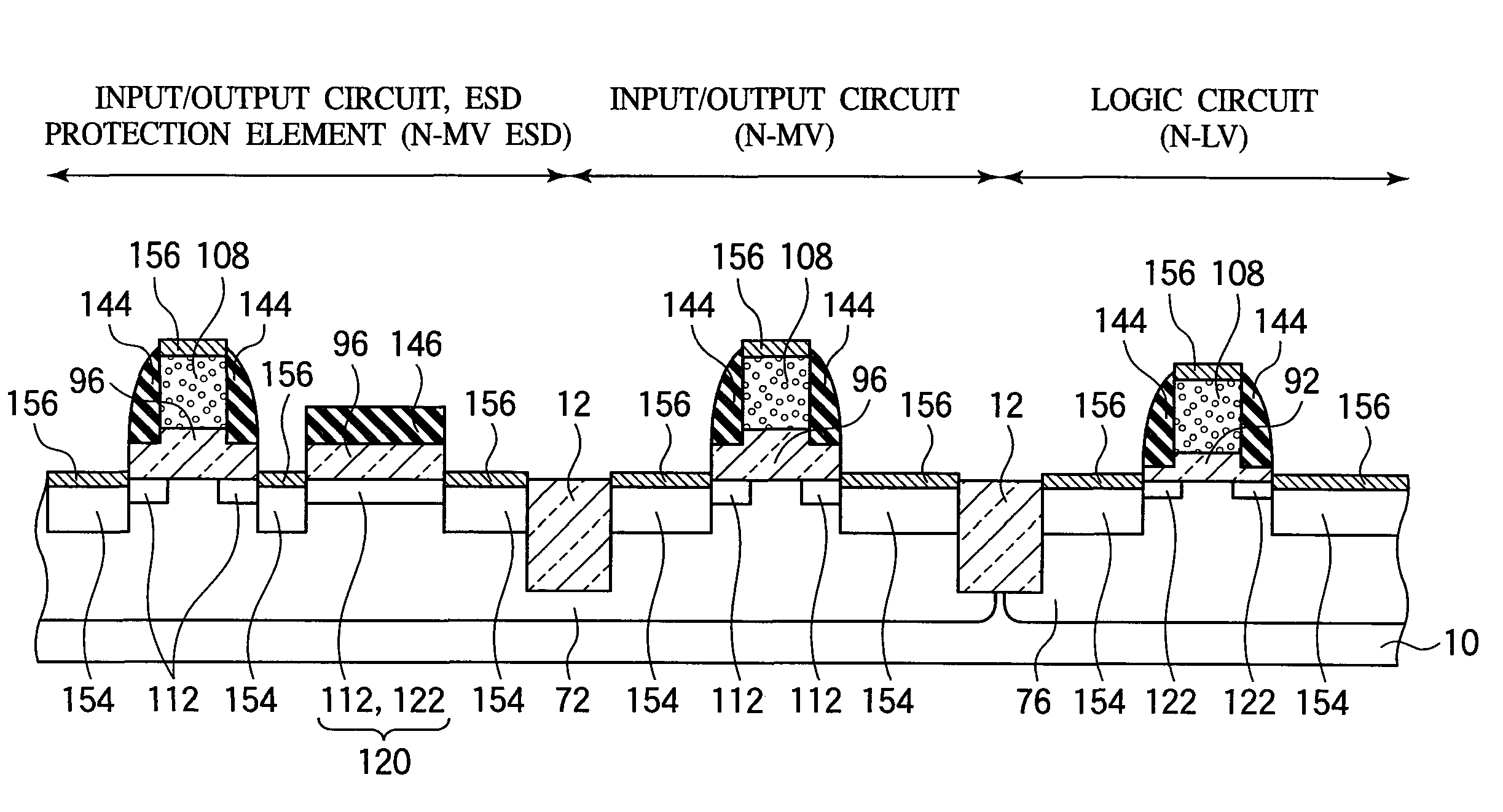
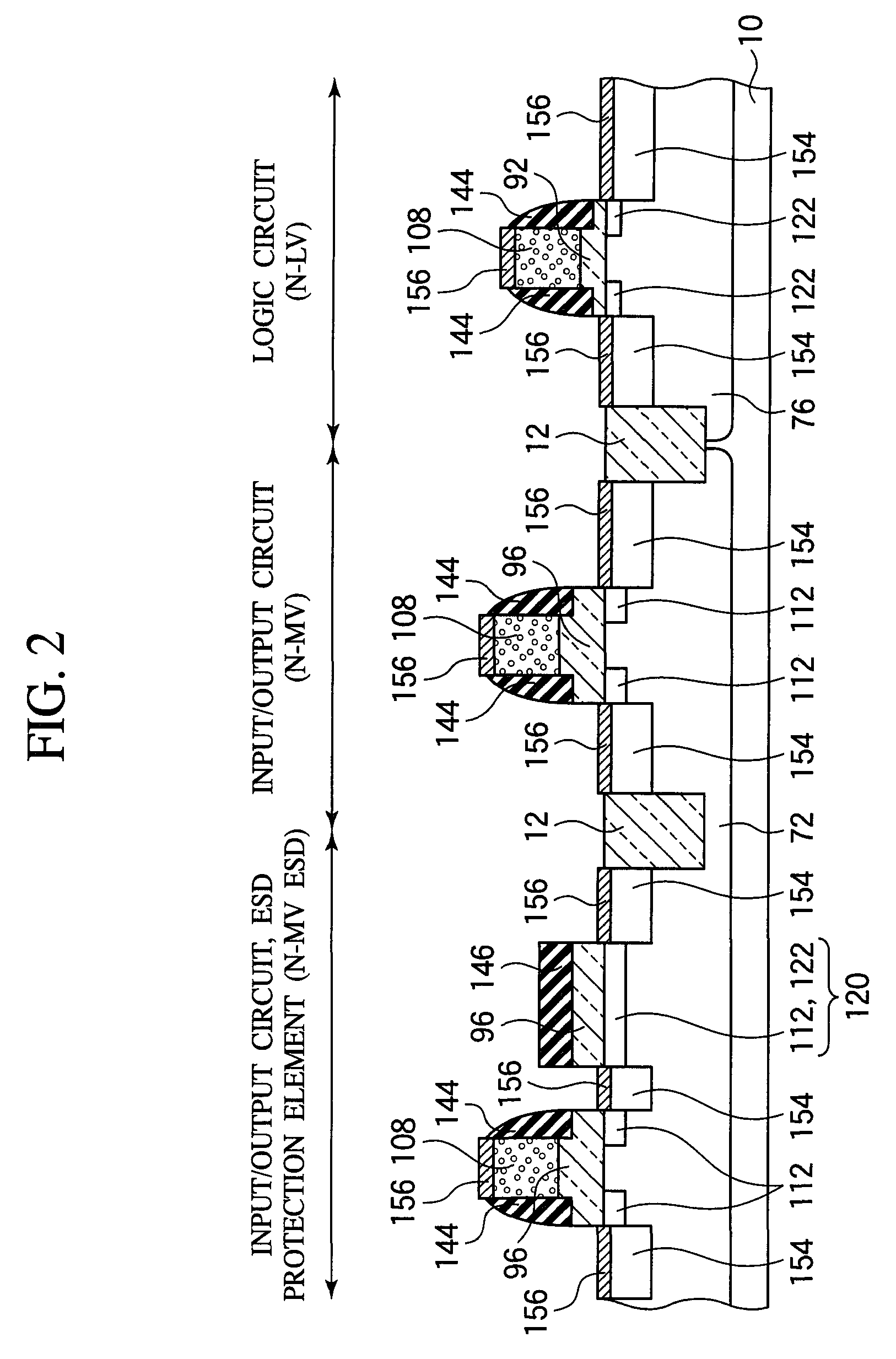
The semiconductor device and the method of manufacturing the same according to a first embodiment of the present invention will be explained with reference to FIGS. 1 to 7B.
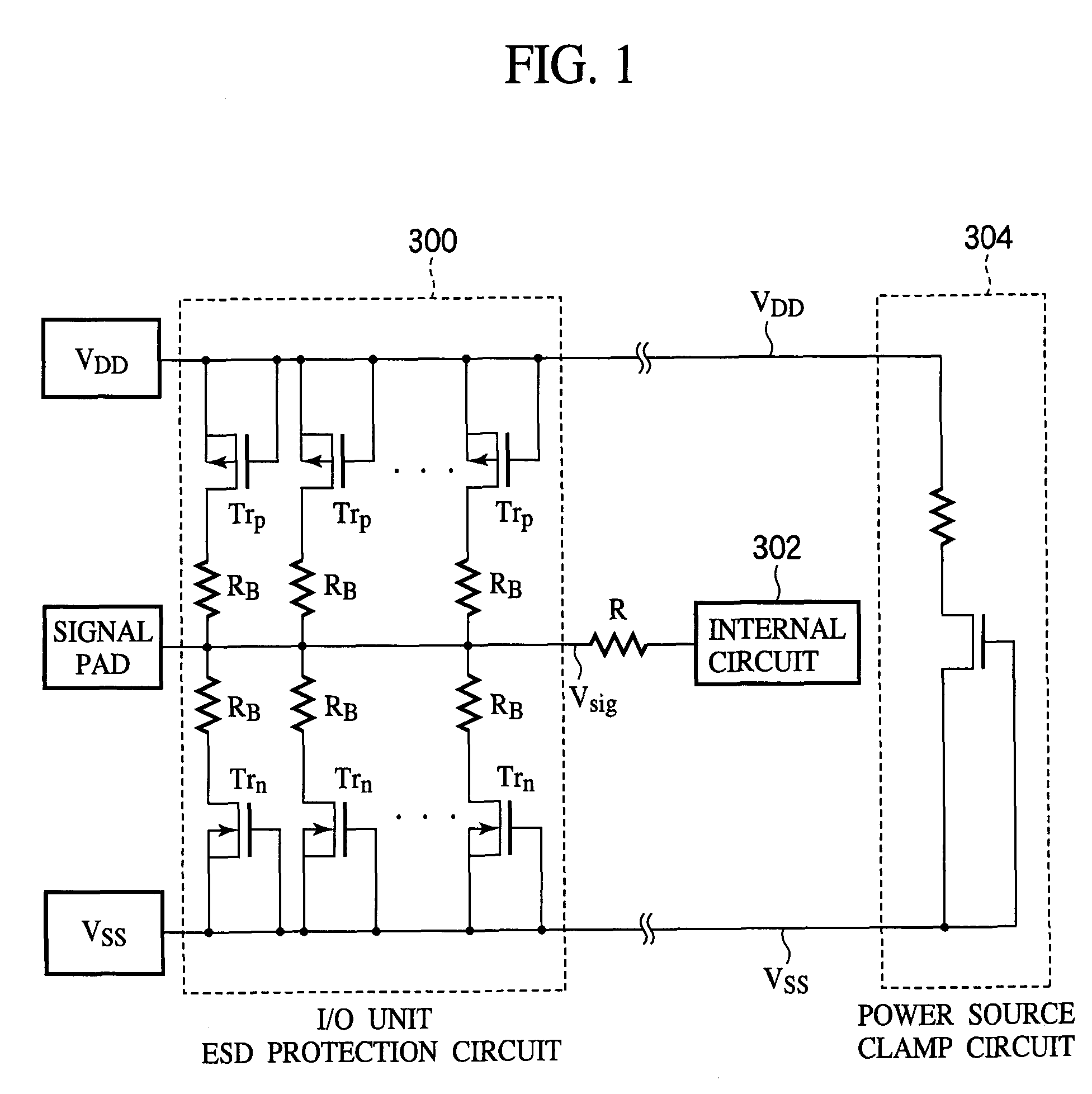
FIG. 1 is a circuit diagram of one example of the ESD protection circuit using MIS transistors including ballast resistors. FIG. 2 is a diagrammatic sectional view showing the structure of the semiconductor device according to the present embodiment. FIG. 3A-7B are sectional views showing the method of manufacturing the semiconductor device according to the present embodiment.
First, the ESD protection circuit using MIS transistors including ballast resistors will be explained with reference to FIG. 1. FIG. 1 shows one example of the ESD protection circuit of the I / O unit.
Between a VDD line and a signal line Vsig, a plurality of p-channel MIS transistors TrP each having a ballast resistor RB are parallelly connected. The p-channel MIS transistor TrP having the ballast resistor RB is a p-channel M...
second embodiment
A Second Embodiment
The semiconductor device and the method of manufacturing the same according to a second embodiment of the present invention will be explained with reference to FIGS. 8 to 21B. The same members of the present embodiment as those of the semiconductor device and the method of manufacturing the same according to the first embodiment shown in FIGS. 2 to 7B are represented by the same reference numbers not to repeat or to simplify their explanation.
FIG. 8 is a graph showing the depth-wise distribution of the impurity concentration of the extension region. FIG. 9 is a diagrammatic sectional view showing the structure of the semiconductor device according to the present embodiment. FIGS. 10A-20B are sectional views showing the method of manufacturing the semiconductor device according to the present embodiment. FIGS. 21A and 21B are views showing the effects of the semiconductor device and the method of manufacturing the same according to the present embodiment.
In the fir...
third embodiment
A Third Embodiment
The semiconductor device and method of manufacturing the same according to a third embodiment of the present invention will be explained with reference to FIGS. 22 to 40B. The same members of the present embodiment as those of the semiconductor device and the method of manufacturing the same according to the first and the second embodiments are represented by the same reference numbers not to repeat or to simplify their explanation.
FIG. 22 is a diagrammatic sectional view showing the structure of the semiconductor device according to the present embodiment. FIGS. 23A to 40B are sectional views showing the method of manufacturing the semiconductor device according to the present embodiment.
In the present embodiment, the present invention is applied to a semiconductor combined with a flash memory.
First, the structure of the semiconductor device according to the present embodiment will be explained with reference to FIG. 22.
In a silicon substrate 10, a device isolatio...
PUM
 Abstract
Description
Claims
Application Information