Interconnect device with discrete in-line components

a technology of discrete components and sockets, which is applied in the direction of printed circuit aspects, electronic products manufacture, electrical apparatus, etc., can solve the problems of increasing the chances of spurious and interfering emissions signals being created, increasing the chance of spurious and interfering emissions signals, and raising issues with respect to impedance matching between device pins and connections

Active Publication Date: 2011-02-22
SANGOMA US INC
View PDF21 Cites 31 Cited by
  • Summary
  • Abstract
  • Description
  • Claims
  • Application Information

AI Technical Summary

Benefits of technology

[0010]An interconnect device is provided with a body through which one or more wells have been provided. A two-terminal component is positioned in one or more of the wells. The component is sealed in its respective well such that the two terminals are accessible on opposite sides of the body. The body corresponds to a Ball Grid Array (BGA) device and each well corresponds with a solder ball of the BGA device and a pad on a printed circuit board (PCB). The body is positioned between the BGA device and PCB. The component in the well is then inline with the solder ball on the BGA device and the corresponding pad on the PCB. Providing the component in the well frees up surface area on the PCB and also allows for positioning the two-terminal component closer to a signal source from the BGA device. The terminals of the component may be solderable or made from a conductive pliable material and may be spring-mounted on the component.

Problems solved by technology

The ever increasing complexity of today's electronic devices has led to more complex circuits being provided in smaller packages.
Faster system clock speeds increase the chances of spurious and interfering emissions signals being created as well as raise issues with respect to impedance matching between device pins and connections.
Despite the already small size of these components, the drive toward ever smaller electronic devices, e.g., cell phones and cameras, and thus, smaller and more densely populated printed circuit boards, makes placement of even passive SMT components on printed circuit boards challenging.
The Ball Grid Array (BGA) device presents issues when a terminating device, e.g., a resistor, needs to be connected and placed nearby.
This limited space creates a challenge for optimal component placement.
The trace 2110b, however, forms an extra stub length that can add undesirable inductance, thus possibly affecting performance or causing spurious noise, but which is required to connect the surface mount resistor 1100 to the BGA device 1110.
Thus, the presence of the buried component on the signal layer still requires valuable via and signal trace space on the inner layers of the board.

Method used


Image

  • Interconnect device with discrete in-line components
  • Interconnect device with discrete in-line components
  • Interconnect device with discrete in-line components

Examples


Embodiment Construction

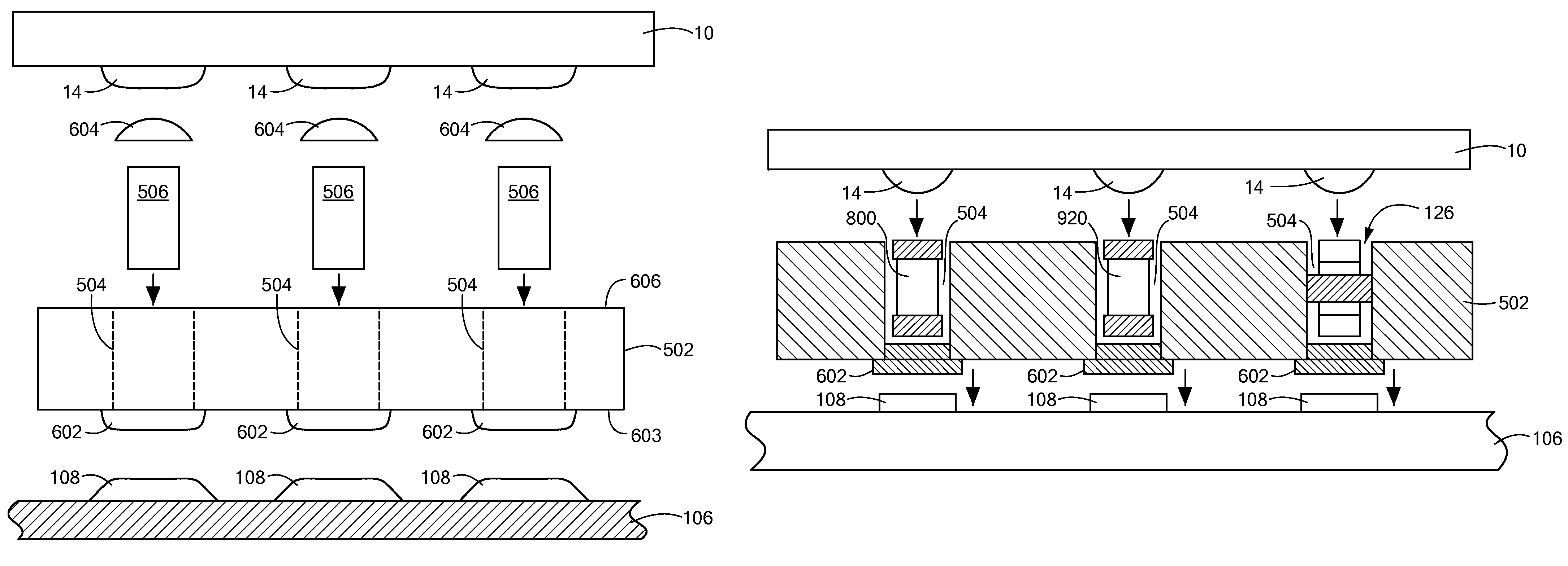
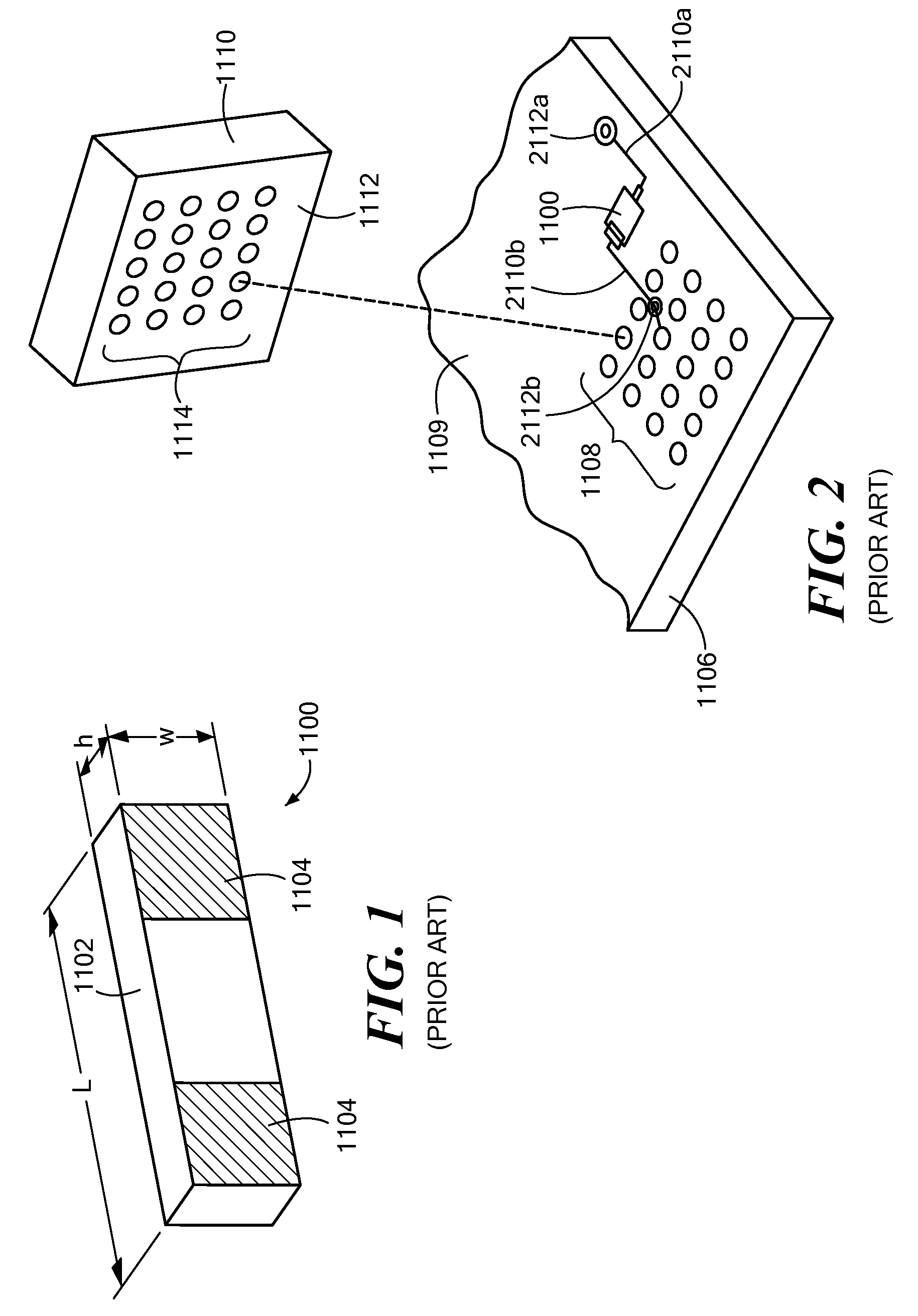
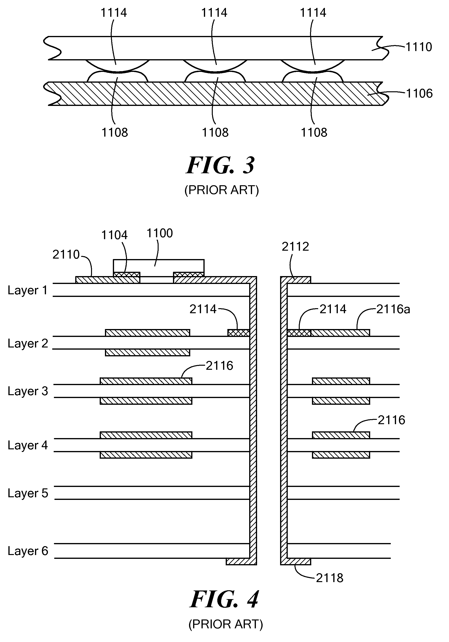
[0029]It is to be appreciated that embodiments of the methods and apparatuses discussed herein are not limited in application to the details of construction and the arrangement of components set forth in the following description or illustrated in the accompanying drawings. The methods and apparatuses are capable of implementation in other embodiments and of being practiced or of being carried out in various ways. Examples of specific implementations are provided herein for illustrative purposes only and are not intended to be limiting. In particular, acts, elements and features discussed in connection with any one or more embodiments are not intended to be excluded from a similar role in any other embodiments. Also, the phraseology and terminology used herein is for the purpose of description and should not be regarded as limiting. The use herein of “including,”“comprising,”“having,”“containing,”“involving,” and variations thereof, is meant to encompass the items listed thereafter ...


PUM


Abstract

An interconnect device is provided with a body through which a plurality of wells has been defined. At least one component having two terminals is provided in one or more of the wells. The component is sealed in its respective well such that the two terminals are accessible on opposite sides of the body. The body corresponds to a Ball Grid Array (BGA) device and is positioned between a BGA device and a printed circuit board (PCB). The component in the well is then inline with a solder ball on the BGA device and a corresponding pad on the PCB. Providing the component in the well frees up surface area on the PCB and also allows for positioning the component closer to a source of a signal. A component in the well is a discrete component having two terminals that may be solderable or made from a conductive pliable material. The terminals may be spring-mounted on the component.

Description

FIELD OF THE INVENTION[0001]The present invention relates generally to sockets for devices and printed circuit boards and, more particularly, to discrete components provided in a socket.BACKGROUND OF THE INVENTION[0002]The ever increasing complexity of today's electronic devices has led to more complex circuits being provided in smaller packages. Faster system clock speeds increase the chances of spurious and interfering emissions signals being created as well as raise issues with respect to impedance matching between device pins and connections. Signal lines are, at times, terminated with appropriate devices such as resistors or capacitors in order to match impedance and other passive components are provided in order to reduce transients and spurious signal transmissions. It is often desirable to locate the terminating or impedance matching device as close as possible to the signal source or load.[0003]Surface mount (SMT) passive components, such as resistors, capacitors and induct...

Claims


Application Information

Patent Timeline
Patent Type & Authority Patents(United States)
IPC IPC(8): H01R12/00H01R12/51
CPCH05K1/023H05K1/0246H05K1/181H01R12/52Y02P70/611H05K1/0233H05K1/141H05K1/184H05K3/4046H05K2201/10022H05K2201/10037H05K2201/10174H05K2201/10181H05K2201/10265H05K2201/10378H05K2201/10734H05K1/0231Y02P70/50
Inventor FRASCO, GARY D.
Owner SANGOMA US INC
Why Eureka
Try Eureka