Photovoltaic solar cell

a solar cell and photovoltaic technology, applied in the field of photovoltaic solar cells, can solve the problems of overlapping marginal conditions and attendants, reducing efficiency, etc., and achieve the effects of improving process efficiency, precise positioning, and increasing process complexity or cos

Inactive Publication Date: 2011-02-22
HELMHOLTZ ZENT BERLIN FUER MATERIALIEN & ENERGIE GMBH
View PDF13 Cites 2 Cited by
  • Summary
  • Abstract
  • Description
  • Claims
  • Application Information

AI Technical Summary

Benefits of technology

[0006]Accordingly, the object of the invention is to be seen as so further to improve the photovoltaic solar cell described supra that a further improvement in the efficiency of the photovoltaic energy conversion can be achieved with two solid material contacts. In this connection, a preferred method of fabricating such a highly efficient solid-material solar cell is to be economical and energy conserving.SUMMARY OF THE INVENTION
[0009]In the solid material solar cell metal nano emitters are used with a predetermined homogenous density distribution dependent upon the occurring minority carriers or their length of diffusion in the semiconductor, thus ensuring minimum use of material at an optimum freedom from shadows of the absorbing semiconductor layer by the second solid material contact and minimum recombination losses. Thus a high conversion efficiency can be achieved in the current collection. In accordance with the invention, the current collection is further significantly improved by the metal nano emitters being now structured three-dimensionally in an acicular or rib-like manner and penetrating deeply into the semiconductor layer. By contrast, the metal nano emitters of the prior art are two-dimensionally structured in a dotted fashion and are present only at the surface of the absorbing semiconductor. Also, the depth of penetration of the metal nano emitters in accordance with the invention can be precisely calculated as a function of the relevant parameters of length of diffusion L, space charge zone w and layer thickness dHL of the semiconductor layer, and can thus be optimized. In accordance with an advantageous embodiment of the invention the metal nano emitters in the semiconductor layer may have lateral branches thus resulting in a tree-like structure. Furthermore, they may extend obliquely within the semiconductor layer so that all regions of the layer may be optimally reached by the nano emitters. Thus, in the solar cell in accordance with the invention, the entire layer thickness of the absorbing semiconductor layer up to the rear contact may be used for energy conversion thus yielding optimum efficiency in the collection of the light-generated minority carriers while avoiding recombination effects. Dotted nano emitters can only achieve a depth of penetration as a function of the simple length of diffusion so that for taking up the entire absorbing semiconductor layer it must be structured correspondingly thin. On the other hand, for light collection of approximately 90% the layer thickness of the semiconductor layer has to be greater than three times the absorption length 1 / α with the coefficient of absorption α which may lead to overlapping marginal conditions and attendant lower efficiency.
[0010]In consequence of the penetration into the depth of the absorbing semiconductor layer, the invention makes possible the use of semiconductor materials which are not of first class quality, i.e. materials of lesser diffusion length of the minority carriers. This results in a noticeable cost reduction. Furthermore, crystalline materials and epitaxially grown layers of, for instance, Si, GaAs and InP may be made significantly thinner in view of the fact that in the solar cell in accordance with the invention the red sensitivity in the collection near the rear contact is significantly improved. This is particularly true if, in accordance with one embodiment of the invention a reflective layer is applied to the rear surface of the semiconductor layer in front of the rear contact. According to a further embodiment of the invention a further improvement of the conversion efficiency results from applying an antireflection coating to the transparent conductive layer. This may be, for instance, a layer with a positive or negative pyramidal structure or with some other micro-structuring which safely catches impinging light and conducts it to the absorber.
[0020]Precise positioning and maintaining the dimensions of the nano emitters by precisely structuring the oxide layer and the semiconductor layer are important as regards improving the efficiency of the solar cell with specially structured metal nano emitters described supra. In technological applications, the oxide layer may be structured, for instance, by electron beam lithography or by ion beam etching (FIB=focused ion beam etching). Alternatively, but still without applying high temperatures, the oxide layer, which may consist of ZnO, SnO2 or ITO, may be structured, in accordance with a further embodiment of the process, by scanning probe microscopy which would result in a still more precise and controlled definition of the nano emitter positions. In this context, two basic possibilities exist: On the one hand the oxide layer may be scanned in a selected surface area by AFM (atomic force microscopy) with a sufficiently high hold-down force. This process results in the oxide layer being correspondingly shifted laterally and in the semiconductor layer disposed under it to be exposed. On the other hand it is possible by means of AFM to form an indentation with a diamond needle by which the oxide layer is penetrated for the formation of a contact. In accordance with a further embodiment of the invention it is also possible in mechanically structuring the oxide layer to provide a plurality of indentations by parallel embossing for structuring an oxide layer of large surface. By this so-called millipede technique a large number (several hundred) of indentations are simultaneously carried out by AFM (atomic force microscopy), for instance. For large-scale applications in particular such structuring is of particular interest in connection with a large-scale continuous electrochemical / wet-chemical fabrication. In order to cure deformations possibly occurring during the indenting or scratching, the structures, in accordance with a further embodiment of the method, may subsequently be subjected to careful chemical or electrochemical etching of the positions of the removed oxide layer followed by a potential, current or charge-controlled application of an electrically insulating anodic oxide layer (1 to 3 atom layers) on the structure of the semiconductor layer prior to precipitation of metal. This process serves to suppress recombination processes at and in the vicinity of defects.
[0021]The surface structuring of the oxide layer is followed by a process step for deepening the structures into the semiconductor layer. This is carried out by wet-chemical or electrochemical or photo-electrochemical etching. Commencing from dot structures in the oxide layer, there will result acicular or porous recesses. Linear structures in the oxide layer are deepened to ribs or troughs. The etching is a simple yet precise operation since the surface of the semiconductor which is not to be etched is securely protected by the oxide layer. The depth of etching may be precisely defined by the corresponding parameters of material and time. The same is true in respect of possible etching of lateral branches which may proceed from the central acicular or rib-like etching recesses, as well as of recesses extending obliquely within the semiconductor layer. An importance process step is the subsequent filling of the acicular or rib-like recesses and of possible lateral branches, i.e. the local precipitation of the metal nano emitters. In this connection, a light-induced or potential-controlled electrochemical precipitation of metal is carried out. The precipitation in the lateral can be safely ensured. In connection with light precipitation the metal is selected such that a rectifying Schottky contact results. The semiconductor may be p-doped or n-doped or not be doped at all. In the case of n-semiconductors the metal precipitation occurs in the dark by forming negative accumulation layers. To prevent repetitions, reference is made to the specific description in connection with the corresponding drawings as regards the precise operation during the light-induced precipitation. An alternative preparation may be carried out by introducing a metallic colloid into the acicular or rib-like recesses in the semiconductor layer. After introduction of the colloid the exposed surface areas of the semiconductor layer are electrochemically oxidized so that the desired nano emitter structure is then embedded in an oxide layer. Process steps following the formation of the nano emitters may in further embodiments include the application of a reflexive layer on the rear surface of the semiconductor layer and / or the application of an antireflective layer on the transparent conductive layer. Both of these additional layers serve further to improve the efficiency as has already be set forth in connection with the solar cell in accordance with the invention.

Problems solved by technology

On the other hand, for light collection of approximately 90% the layer thickness of the semiconductor layer has to be greater than three times the absorption length 1 / α with the coefficient of absorption α which may lead to overlapping marginal conditions and attendant lower efficiency.

Method used


Image

  • Photovoltaic solar cell
  • Photovoltaic solar cell
  • Photovoltaic solar cell

Examples


Embodiment Construction

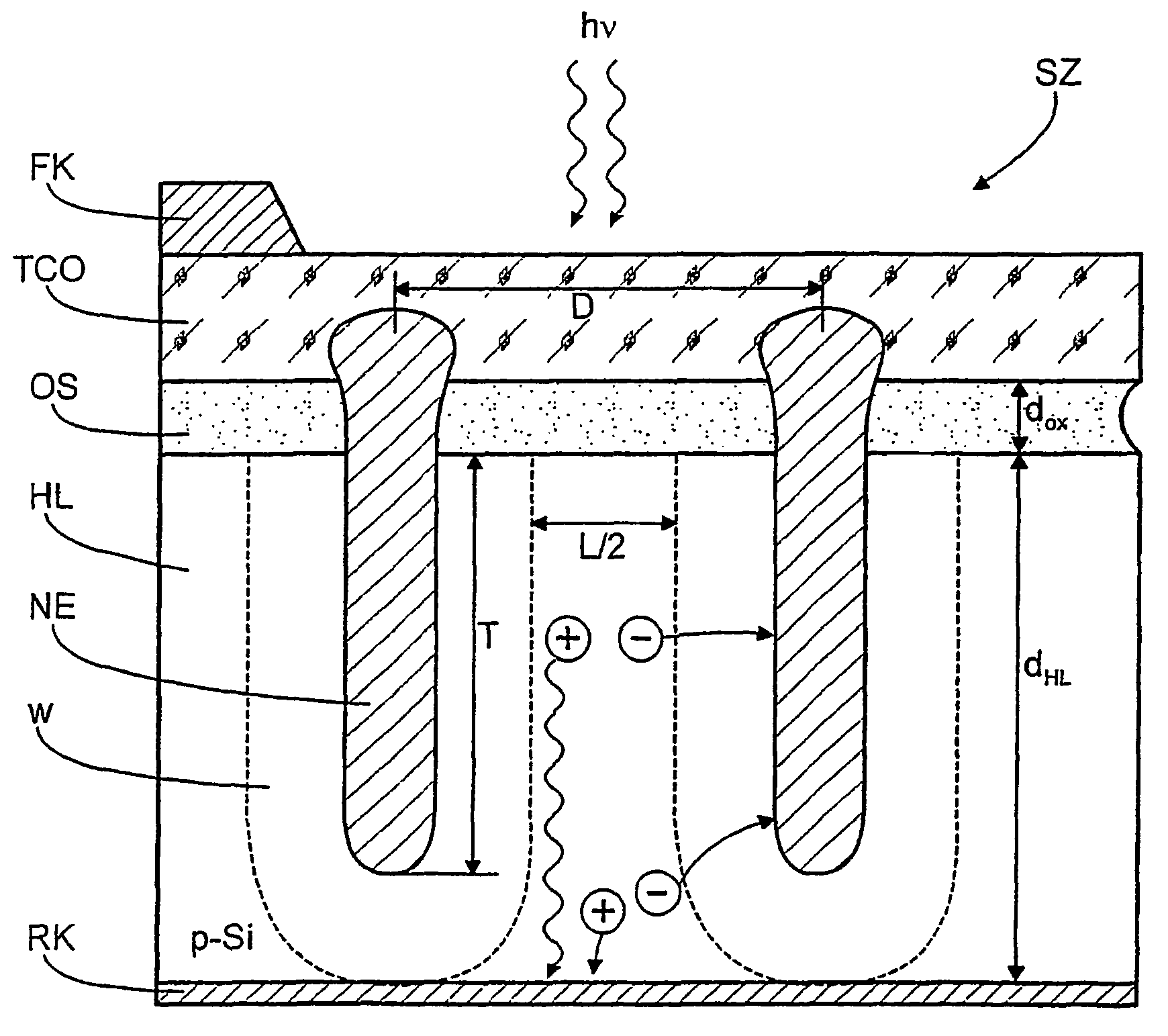
[0027]FIG. 1 depicts a photovoltaic solar cell SZ having an electrical solid material contact between a doped semiconductor layer HL of layer thickness dHL and a plurality of metal nano emitters NE embedded in an electrically insulating oxide layer OS on the surface of the semiconductor layer HL. Given an appropriate selection of the metal there will result a rectifying Schottky contact with the semiconductor layer HL. In the semiconductor layer HL the rectifying nano emitters NE generate a space charge zone (depleted range) of extent w. Upon exposure, provided the impinging light energy hv is greater than the work function Eg of the charge carriers, pairs of electron holes will be formed in the semiconductor layer HL. The minority carrier (electrons for p-silicon as the semiconductor, holes or “defect electrons” for n-silicon) migrate at a diffusion length L to the metal nano emitters NE acting as a sink. A particularly efficient conversion of solar energy will be achieved if the d...


PUM


Abstract

A photovoltaic solar cell (SZ) of improved light-to-current conversion properties is provided with nano emitters (NE) of acicular or rib-like form and are separated from each other at a uniform distance D≦√{square root over (2)}L and penetrating to a penetration depthT≥dHL-L2+winto the semiconductor layer (HL).

Description

BACKGROUND OF THE INVENTION[0001]1. Field of the Invention[0002]The invention relates to a photovoltaic solar cell with an electrical solid material contact between a semiconductor layer of a layer thickness of dHL and with a plurality of metal nano emitters embedded in an electrically insulating oxide layer disposed on the semiconductor layer and each provided with a space-charge region of dimension w within the semiconductor layer to which the minority carriers migrate over a diffusion length L, and with a transparent conductive layer electrically insulated from the semiconductor layer by the oxide layer as well as with front and rear contacts, and to a method of manufacturing such a solar cell.[0003]2. The Prior Art[0004]In photovoltaic current generation the efficiency of the conversion of impinging sun light to electrical current is of the utmost importance. In order to obtain an optimum yield, aside from reducing losses of reflection and recombination, particular efforts are m...

Claims


Application Information

Patent Timeline
Patent Type & Authority Patents(United States)
IPC IPC(8): H01L31/00
CPCH01L31/022425H01L31/07H01L31/1884H01L31/1804Y02P70/521Y02E10/547Y02P70/50
Inventor LEWERENZ, HANS-JOACHIM
Owner HELMHOLTZ ZENT BERLIN FUER MATERIALIEN & ENERGIE GMBH
Why Eureka
Try Eureka