[0006] Accordingly, the object of the invention is to be seen as so further to improve the
photovoltaic solar cell described supra that a further improvement in the efficiency of the
photovoltaic energy conversion can be achieved with two
solid material contacts. In this connection, a preferred method of fabricating such a highly efficient
solid-material
solar cell is to be economical and energy conserving. SUMMARY OF THE INVENTION
[0008] In the
solid material solar cell metal nano emitters are used with a predetermined homogenous
density distribution dependent upon the occurring minority carriers or their length of
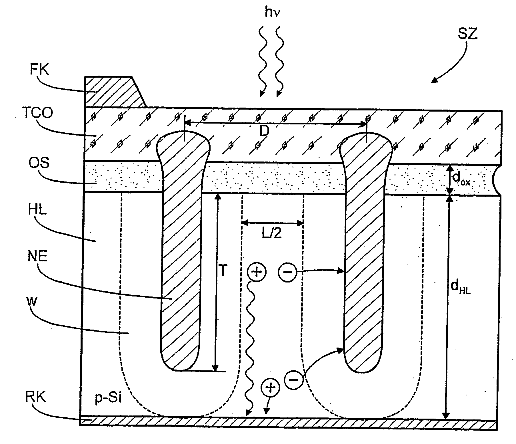
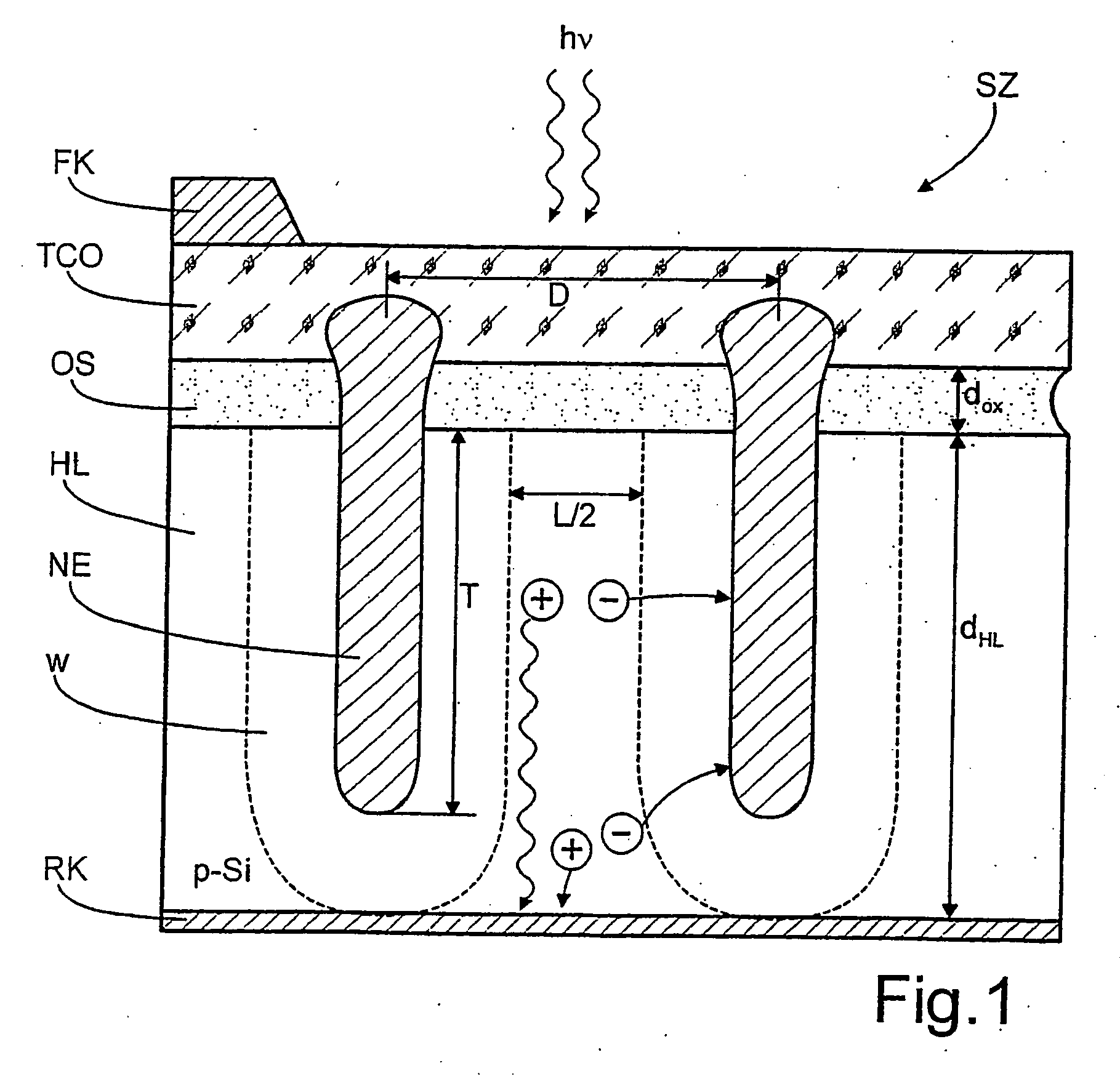
diffusion in the semiconductor, thus ensuring minimum use of material at an optimum freedom from shadows of the absorbing semiconductor layer by the second
solid material contact and minimum recombination losses. Thus a high conversion efficiency can be achieved in the current collection. In accordance with the invention, the current collection is further significantly improved by the
metal nano emitters being now structured three-dimensionally in an
acicular or rib-like manner and penetrating deeply into the semiconductor layer. By contrast, the metal nano emitters of the prior art are two-dimensionally structured in a dotted fashion and are present only at the surface of the absorbing semiconductor. Also, the
depth of penetration of the metal nano emitters in accordance with the invention can be precisely calculated as a function of the relevant parameters of length of
diffusion L,
space charge zone w and
layer thickness dHL of the semiconductor layer, and can thus be optimized. In accordance with an advantageous embodiment of the invention the metal nano emitters in the semiconductor layer may have lateral branches thus resulting in a tree-like structure. Furthermore, they may extend obliquely within the semiconductor layer so that all regions of the layer may be optimally reached by the nano emitters. Thus, in the solar
cell in accordance with the invention, the entire layer thickness of the absorbing semiconductor layer up to the rear contact may be used for energy conversion thus yielding optimum efficiency in the collection of the light-generated minority carriers while avoiding recombination effects. Dotted nano emitters can only achieve a
depth of penetration as a function of the simple length of diffusion so that for taking up the entire absorbing semiconductor layer it must be structured correspondingly thin. On the other hand, for light collection of approximately 90% the layer thickness of the semiconductor layer has to be greater than three times the absorption length 1 / α with the coefficient of absorption α which may lead to overlapping marginal conditions and attendant lower efficiency.
[0009] In consequence of the penetration into the depth of the absorbing semiconductor layer, the invention makes possible the use of
semiconductor materials which are not of
first class quality, i.e. materials of lesser diffusion length of the minority carriers. This results in a noticeable cost reduction. Furthermore,
crystalline materials and epitaxially grown
layers of, for instance, Si, GaAs and InP may be made significantly thinner in view of the fact that in the solar
cell in accordance with the invention the red sensitivity in the collection near the rear contact is significantly improved. This is particularly true if, in accordance with one embodiment of the invention a
reflective layer is applied to the rear surface of the semiconductor layer in front of the rear contact. According to a further embodiment of the invention a further improvement of the conversion efficiency results from applying an
antireflection coating to the transparent conductive layer. This may be, for instance, a layer with a positive or negative pyramidal structure or with some other micro-structuring which safely catches impinging light and conducts it to the absorber.
[0019] Precise positioning and maintaining the dimensions of the nano emitters by precisely structuring the
oxide layer and the semiconductor layer are important as regards improving the efficiency of the solar
cell with specially structured metal nano emitters described supra. In technological applications, the oxide layer may be structured, for instance, by
electron beam
lithography or by
ion beam
etching (FIB=
focused ion beam etching). Alternatively, but still without applying high temperatures, the oxide layer, which may consist of ZnO, SnO2 or ITO, may be structured, in accordance with a further embodiment of the process, by
scanning probe microscopy which would result in a still more precise and controlled definition of the nano emitter positions. In this context, two basic possibilities exist: On the one hand the oxide layer may be scanned in a selected surface area by AFM (
atomic force microscopy) with a sufficiently high hold-down force. This process results in the oxide layer being correspondingly shifted laterally and in the semiconductor layer disposed under it to be exposed. On the other hand it is possible by means of AFM to form an indentation with
a diamond needle by which the oxide layer is penetrated for the formation of a contact. In accordance with a further embodiment of the invention it is also possible in mechanically structuring the oxide layer to provide a plurality of indentations by parallel
embossing for structuring an oxide layer of large surface. By this so-called millipede technique a large number (several hundred) of indentations are simultaneously carried out by AFM (
atomic force microscopy), for instance. For large-scale applications in particular such structuring is of particular interest in connection with a large-scale continuous electrochemical / wet-chemical fabrication. In order to cure deformations possibly occurring during the indenting or
scratching, the structures, in accordance with a further embodiment of the method, may subsequently be subjected to careful chemical or
electrochemical etching of the positions of the removed oxide layer followed by a potential, current or charge-controlled application of an electrically insulating
anodic oxide layer (1 to 3 atom
layers) on the structure of the semiconductor layer prior to
precipitation of metal. This process serves to suppress recombination processes at and in the vicinity of defects.
[0020] The surface structuring of the oxide layer is followed by a process step for deepening the structures into the semiconductor layer. This is carried out by wet-chemical or electrochemical or photo-
electrochemical etching. Commencing from dot structures in the oxide layer, there will result
acicular or porous recesses. Linear structures in the oxide layer are deepened to ribs or troughs. The
etching is a simple yet precise operation since the surface of the semiconductor which is not to be etched is securely protected by the oxide layer. The depth of etching may be precisely defined by the corresponding parameters of material and time. The same is true in respect of possible etching of lateral branches which may proceed from the central acicular or rib-like etching recesses, as well as of recesses extending obliquely within the semiconductor layer. An importance process step is the subsequent filling of the acicular or rib-like recesses and of possible lateral branches, i.e. the local
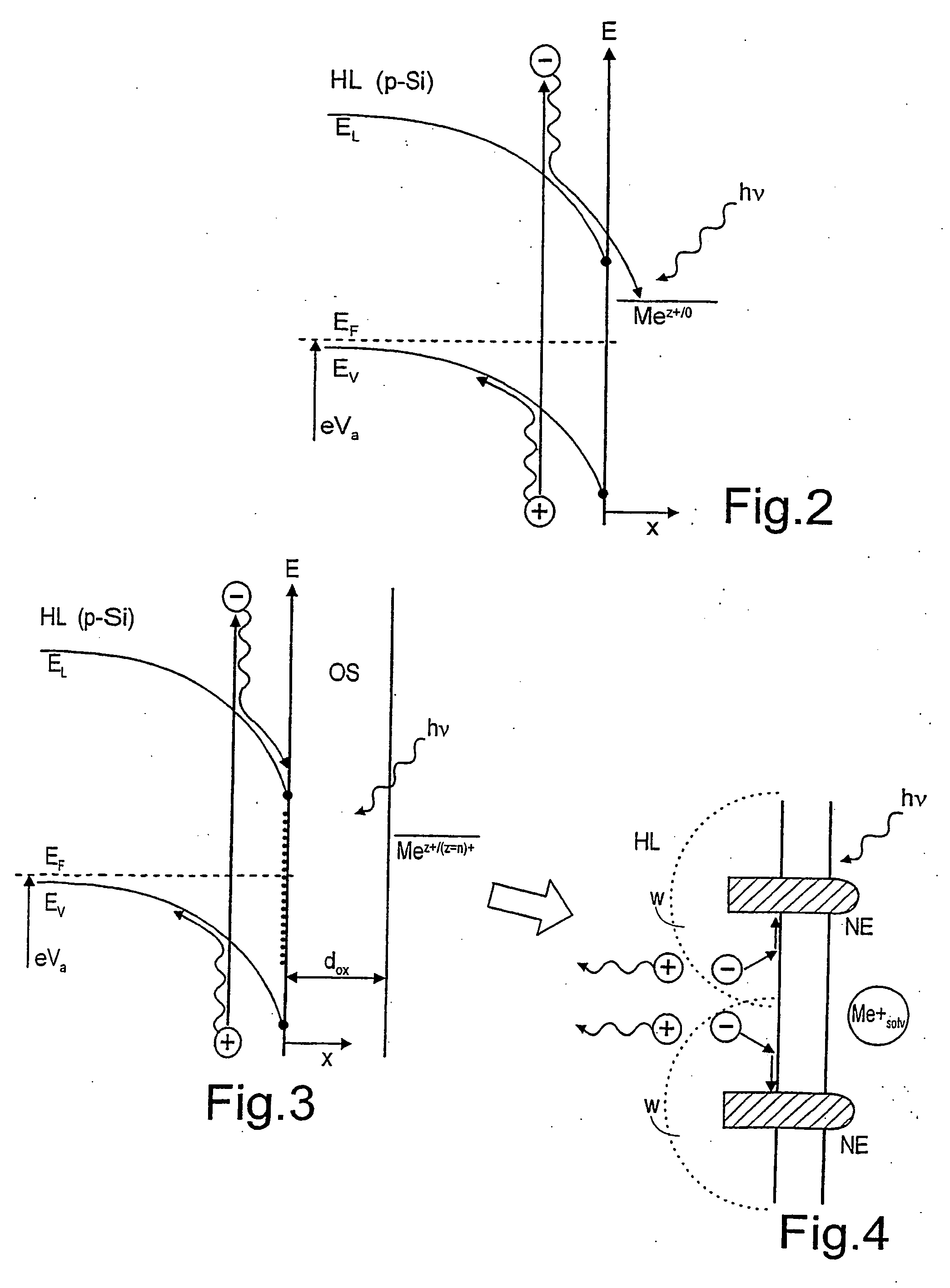
precipitation of the metal nano emitters. In this connection, a light-induced or potential-controlled electrochemical
precipitation of metal is carried out. The precipitation in the lateral can be safely ensured. In connection with light precipitation the metal is selected such that a rectifying Schottky contact results. The semiconductor may be p-doped or n-doped or not be doped at all. In the case of n-semiconductors the
metal precipitation occurs in the dark by forming negative accumulation
layers. To prevent repetitions, reference is made to the specific description in connection with the corresponding drawings as regards the precise operation during the light-induced precipitation. An alternative preparation may be carried out by introducing a metallic
colloid into the acicular or rib-like recesses in the semiconductor layer. After introduction of the
colloid the exposed surface areas of the semiconductor layer are electrochemically oxidized so that the desired nano emitter structure is then embedded in an oxide layer. Process steps following the formation of the nano emitters may in further embodiments include the application of a reflexive layer on the rear surface of the semiconductor layer and / or the application of an antireflective layer on the transparent conductive layer. Both of these additional layers serve further to improve the efficiency as has already be set forth in connection with the solar cell in accordance with the invention.

