Electro-optical device, driving circuit, and electronic apparatus for decreasing frame size

a technology of electronic devices and circuits, applied in the direction of static indicating devices, non-linear optics, instruments, etc., can solve the problems of large transistors, limited exterior design of electronic devices into which a display panel is inserted, and the connection of display panels. to achieve the effect of reducing the frame siz

Active Publication Date: 2011-03-08
JAPAN DISPLAY WEST
View PDF8 Cites 17 Cited by
  • Summary
  • Abstract
  • Description
  • Claims
  • Application Information

AI Technical Summary

Benefits of technology

An advantage of some aspects of the invention is that it provides an electro-optical device, a driving circuit, and an electronic apparatus which can decrease the frame size thereof in a case where the data lines are driven by using a demultiplexer.
According to a first aspect of the invention, there is provided a driving circuit of an electro-optical device that has a plurality of scan lines, a plurality of data lines divided into groups each having m (where m is an integer equal to or greater than two) data lines, and pixels, which are provided in correspondence with intersections of the plurality of scan lines and the plurality of data lines, having gray scale levels in accordance with voltage values of the plurality of data lines at a time when the plurality of scan lines are individually selected and drives the plurality of data lines when one of the plurality of scan lines is selected. The driving circuit includes: first transistors, which are provided in the plurality of data lines, each having one end commonly connected together in each group and the other terminal connected to the data line; second transistors, which are provided in the plurality of data lines, each having one end connected to the data line and the other end commonly connected together in each group; a control circuit that sequentially selects m data lines belonging to each group in a predetermined order at a time when the one of the plurality of scan lines is selected and makes one and the other terminals of the first transistor and the second transistor corresponding to the selected data line be in a mutual conduction state, respectively; a data signal output circuit that outputs data signals having voltage values in accordance with gray scale levels of pixels corresponding to intersections of the one scan line and the selected data line in each group; and operational amplifiers, which are provided in correspondence with the each group, each setting a high voltage value to a voltage supplied to the one terminal of the first transistor in a case where the voltage of the one terminal of the second transistor in the conduction state is lower than a voltage of the data signal output from the data signal output circuit and setting a low voltage value to a voltage supplied to the one terminal of the first transistor in a case where the voltage of the one terminal of the second transistor in the conduction state is lower than the voltage of the data signal output from the data signal output circuit. According to the driving circuit, the operational amplifier circuit controls the voltage value supplied to one terminal of the first transistor such that the voltage of one terminal of the second transistor is identical to the voltage of the data signal output form the data signal output circuit. Accordingly, it is possible to correctly supply a data signal having a voltage value in accordance with the gray scale level, even when the ON resistance between the one and other terminals of the first transistor is high.

Problems solved by technology

The high-definition images can be achieved by increasing the number of scan lines and the number of data lines so as to increase the number of pixels, and in such a case, there is a problem in connections in the display panels.
However, when switching elements constituting the demultiplexer are formed by using transistors, large transistors are required so as to decrease ON resistance of the transistors.
In particular, when the switching elements are formed by amorphous silicon type thin film transistors having a low mobility, very large transistors are required.
Since an area for forming the demultiplexer is an outer frame of a display area, so-called a frame size becomes large, and accordingly, there is a limitation on exterior design of the electronic device into which a display panel is inserted.

Method used


Image

  • Electro-optical device, driving circuit, and electronic apparatus for decreasing frame size
  • Electro-optical device, driving circuit, and electronic apparatus for decreasing frame size
  • Electro-optical device, driving circuit, and electronic apparatus for decreasing frame size

Examples


first embodiment

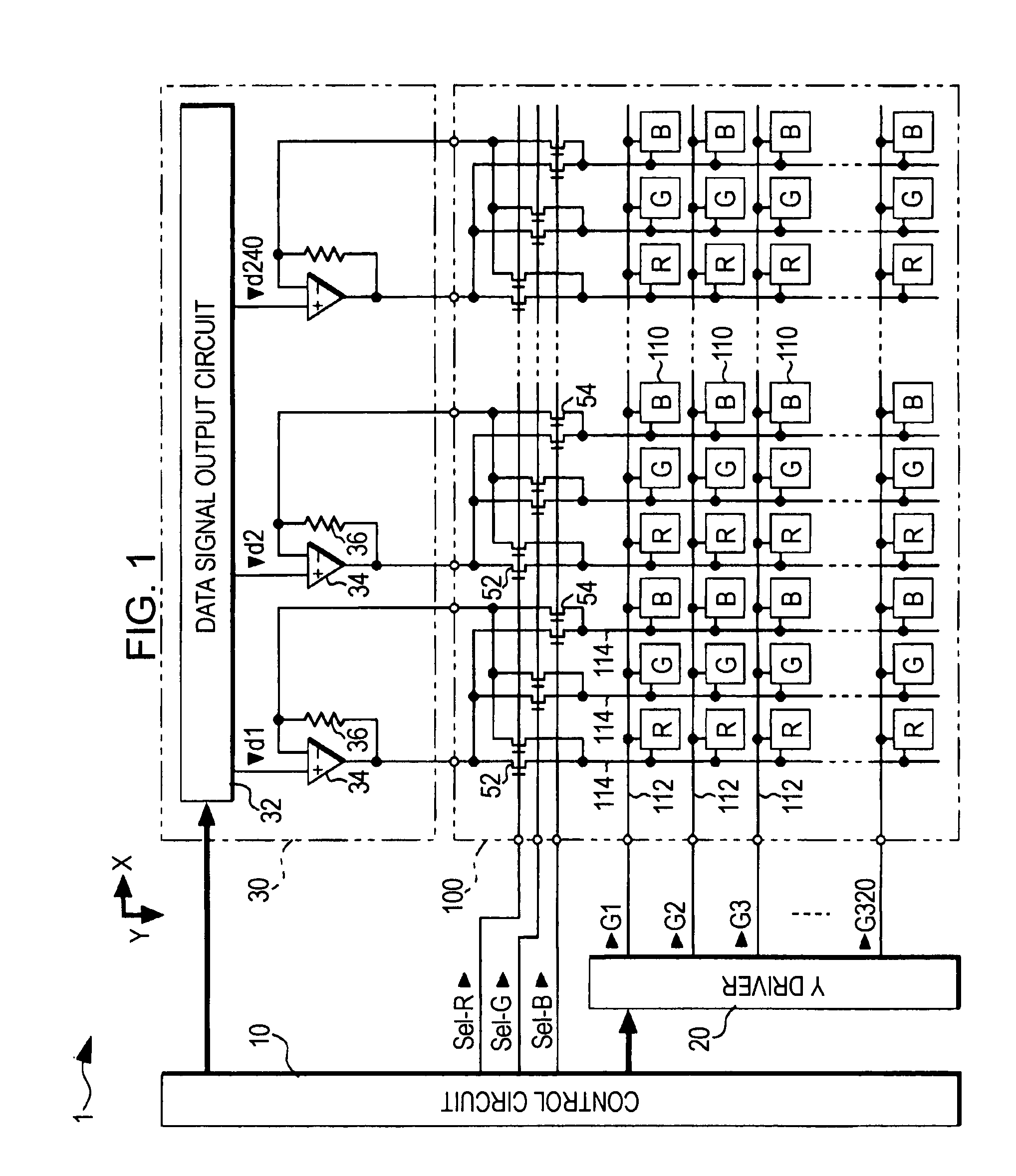
FIG. 1 is a diagram showing the configuration of an electro-optical device according to a first embodiment of the invention.

As shown in the figure, the electro-optical device 1 is basically divided into a control circuit 10, a Y driver 20, an X driver 30, and a display panel 100.

Among these components, the display panel 100, not shown in the figure, has a configuration in which an element substrate and an opposing substrate are disposed together with a constant gap maintained therebetween such that electrode forming surfaces thereof face each other and a liquid crystal is sealed inside the gap. On the element substrate, the Y driver 20 and the X driver 30, which are semiconductor chips, are mounted by using COG (chip on glass) technology or the like. To the Y driver 20, the X driver 30, and the display panel 100, various control signals transmitted from the control circuit 10 are supplied through an FPC (flexible printed circuit) substrate or the like.

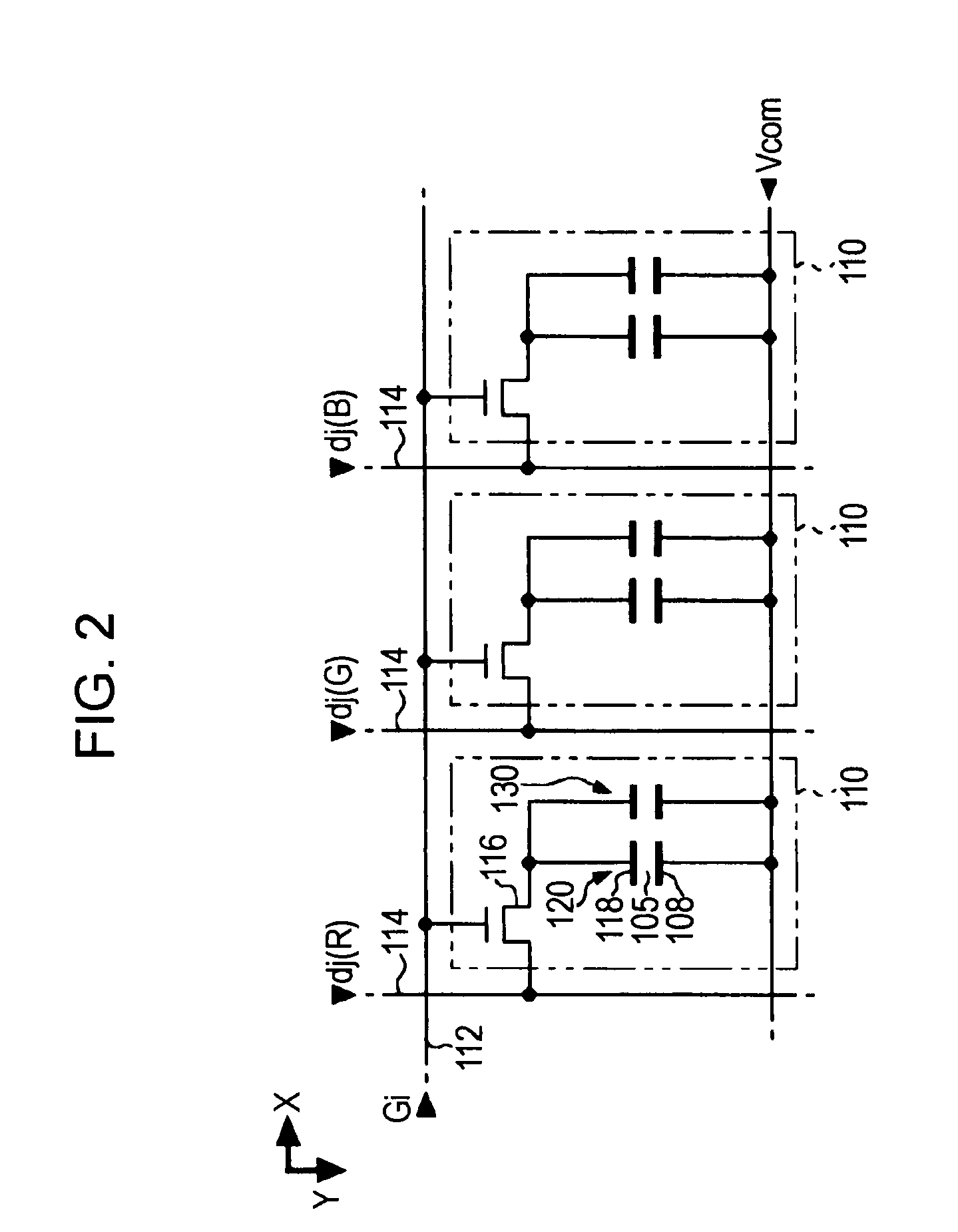
The display panel 100 is divide...

second embodiment

In the above-described first embodiment, the operational amplifier 34 is configured to perform the above-described negative feedback in the whole the period S during which the data signal output circuit 32 outputs a data signal having a voltage value in accordance with the gray scale level.

The data lines 114 have various parasitic capacitances and thus have a characteristic for maintaining the voltage level thereof. Thus, right before the voltage in accordance with the gray scale level is supplied to the data line 114 in the horizontal scan period H during which the i-th scan line is selected, a voltage value in accordance with a display content of the (i−1)-th row, which is one row before the current row, is maintained in the data line 114. Accordingly, there is a case where a change in the voltage of the data line 114 becomes large when the voltage in accordance with the gray scale level is applied in the horizontal scan period H during which the i-th row is selected. In such a ca...

third embodiment

Next, an electro-optical device according to a third embodiment of the invention will be described with reference to FIG. 7.

As shown in the figure, the difference between the second embodiment (see FIG. 4) and the third embodiment is that a switch 40 is disposed for each operational amplifier 34 in the third embodiment.

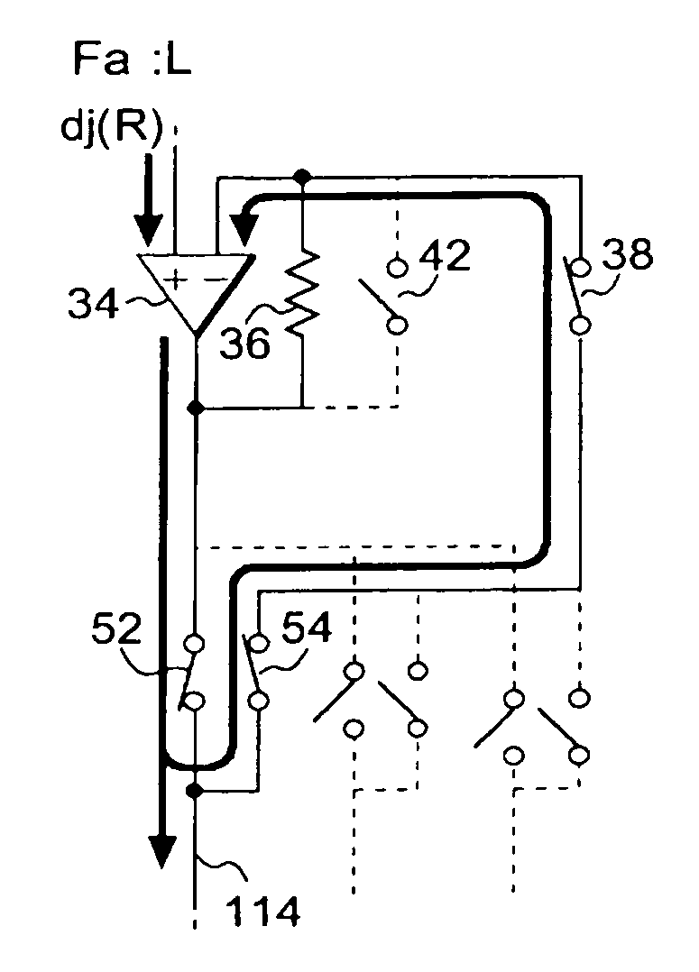
The third embodiment will now be described with primarily focused on the difference. The switch 40 (second switch) is turned on when the signal Fa is level H, and the switch 40 is turned off when the signal Fa is level L. The switch 40 is interposed between the output terminal of the operational amplifier 34 and the common drain electrode of the TFT 54.

Here, for example, when the selection signal Sel-R becomes level H and the signal Fa is level H, as shown in FIG. 8A, the TFTs 52 and 54 corresponding to the data line 114 of color R are turned on, and the switch 38 is turned off and the switch 42 is turned on as in the second embodiment, and accordingly, the operationa...


PUM


Abstract

The object of the present invention is to decrease a frame size in a case where data lines are driven by using a demultiplexer. The data lines 114 are divided into groups each having three data lines. TFTs 52 and 54 are provided for each data line 114, and the TFT 52 between the TFTs has a source electrode commonly connected in each group and a drain electrode connected to the data line 114. In addition, the TFT 54 has a source electrode connected to the data line 114 and a drain electrode commonly connected in each group. A data signal output circuit 32 that outputs data signals having voltage values in accordance with gray scale levels of sub-pixels corresponding to intersections of a selected scan line and a selected data line in each group to each group. Since the selected data line 114 is connected to an inverting input terminal of an operational amplifier 34 through the TFT 54, the operational amplifier 34 controls the voltage of the data line 114 to be identical to the voltage of a signal output from the data signal output circuit.

Description

BACKGROUND1. Technical FieldThe present invention relates to technology for driving data lines using a demultiplexer.2. Related ArtRecently, in electronic devices such as cellular phones or navigation systems, technology for displaying high-definition images has been developed. The high-definition images can be achieved by increasing the number of scan lines and the number of data lines so as to increase the number of pixels, and in such a case, there is a problem in connections in the display panels. For example, when color display of vertical 320 dots×horizontal 240 dots is to be performed, total 720 data lines for 240 dots×3 colors are required in a horizontal direction of the display panel, but when the size of a display image is small, the pitches of the data lines become below the limit for COG (chip on glass) or the like, and accordingly, X drivers that supplies data signals to the data lines cannot be connected to the data lines.Thus, a so-called hybrid method in which the 7...

Claims


Application Information

Patent Timeline
Patent Type & Authority Patents(United States)
IPC IPC(8): G09G3/36
CPCG09G3/3688G09G2300/0426G09G2310/0218G09G2310/0297G09G2330/021G09G3/36G09G3/20G02F1/133
Inventor YAMAZAKI, KATSUNORI
Owner JAPAN DISPLAY WEST
Why Eureka
Try Eureka