Wiring board, semiconductor device using wiring board and their manufacturing methods

a manufacturing method and technology for semiconductor devices, applied in the manufacture of printed circuits, printed circuit aspects, basic electric elements, etc., can solve the problems of unsuitable high-speed signal transmission boards, thin boards cannot meet the current demands for highly dense packaging, and the patterned lines are less accurate, so as to reduce the amount of ultrasonic absorption and reduce the effect of relaxation

Active Publication Date: 2011-03-22
RENESAS ELECTRONICS CORP
View PDF9 Cites 7 Cited by
  • Summary
  • Abstract
  • Description
  • Claims
  • Application Information

AI Technical Summary

Benefits of technology

[0046]According to the present invention, surface wiring layers formed in one surface of an insulating layer with their surface exposed is formed of a first metal film and a second metal film that are stacked in an order in which the first metal film is closer to the one surface of the insulating layer than the second metal film is, and the edges of the first metal film project from the edges of the second metal film in the direction in which the second metal film spreads. This enables the second metal film to be prevented from side etching in the manufacturing process, and enables wiring boards to be manufactured at a high yield even in a case where minute wires equal to or smaller than 50 μm need to be formed on the wiring boards. Hence, it is possible to stably form even wires that are equal to or smaller than 10 μm, which will be in demand from now.
[0047]Since the surface wiring layer formed of the first metal film and the second metal film is embedded in the insulating layer with its surface exposed, it can accept ultrasonical connection manners such as wire bonding while causing less ultrasonic absorption (relaxation) than caused by a wiring structure in which the surface wiring layer protrude from the insulating layer, and can therefore realize stable connection.
[0048]Further, since the surface wiring layer is embedded in the insulating layer, stress applied when a semiconductor device on the wiring board is mounted on another substrate or the like can be absorbed by the whole wiring board, which improves secondary mounting reliability.
[0049]Since the surface wiring layer is formed of the first metal film that is exposed from the one surface of the insulating layer and the second metal film so that the former film is used as a metal film for connection and the latter film is used as a metal film for reducing wire resistance, the area of the connection electrode can be large, and at the same time the second metal film having a low resistance value can have as large a gap as possible from adjacent patterns, which makes it possible to improve connection reliability and to increase resistance to migration between adjacent patterns. Particularly, in a case where the second metal film is made of copper or silver that tends to migrate, migration that is to occur between minute wires can be delayed.
[0050]Further, in the structure where the external surface of the first metal film is located at a position recessed from the one surface of the insulating layer, an effect can be achieved that solder flow is dammed at the time of reflow that accompanies an operation of soldering a semiconductor element such as a flip chip or mounting a solder ball.
[0051]The manufacturing method of a wiring board according to the present invention uses the supporting substrate, which suppresses any deformation during the manufacturing process and gives a fine handling ability. Further, the use of the supporting substrate ensures a thick base and can give a higher accuracy in the alignment of the layers than on a thin manufacturing base.

Problems solved by technology

However, such boards are thick and the through holes make the boards unsuitable for high-speed signal transmission.
However, their manufacturing methods allow them to have only one or two wiring layers, and high elasticity of the tape substrates makes them be patterned less positionally accurately than built-up boards are patterned.
Because of these factors, those thin boards cannot meet the current demands for highly dense packaging.

Method used


Image

  • Wiring board, semiconductor device using wiring board and their manufacturing methods
  • Wiring board, semiconductor device using wiring board and their manufacturing methods
  • Wiring board, semiconductor device using wiring board and their manufacturing methods

Examples


first embodiment

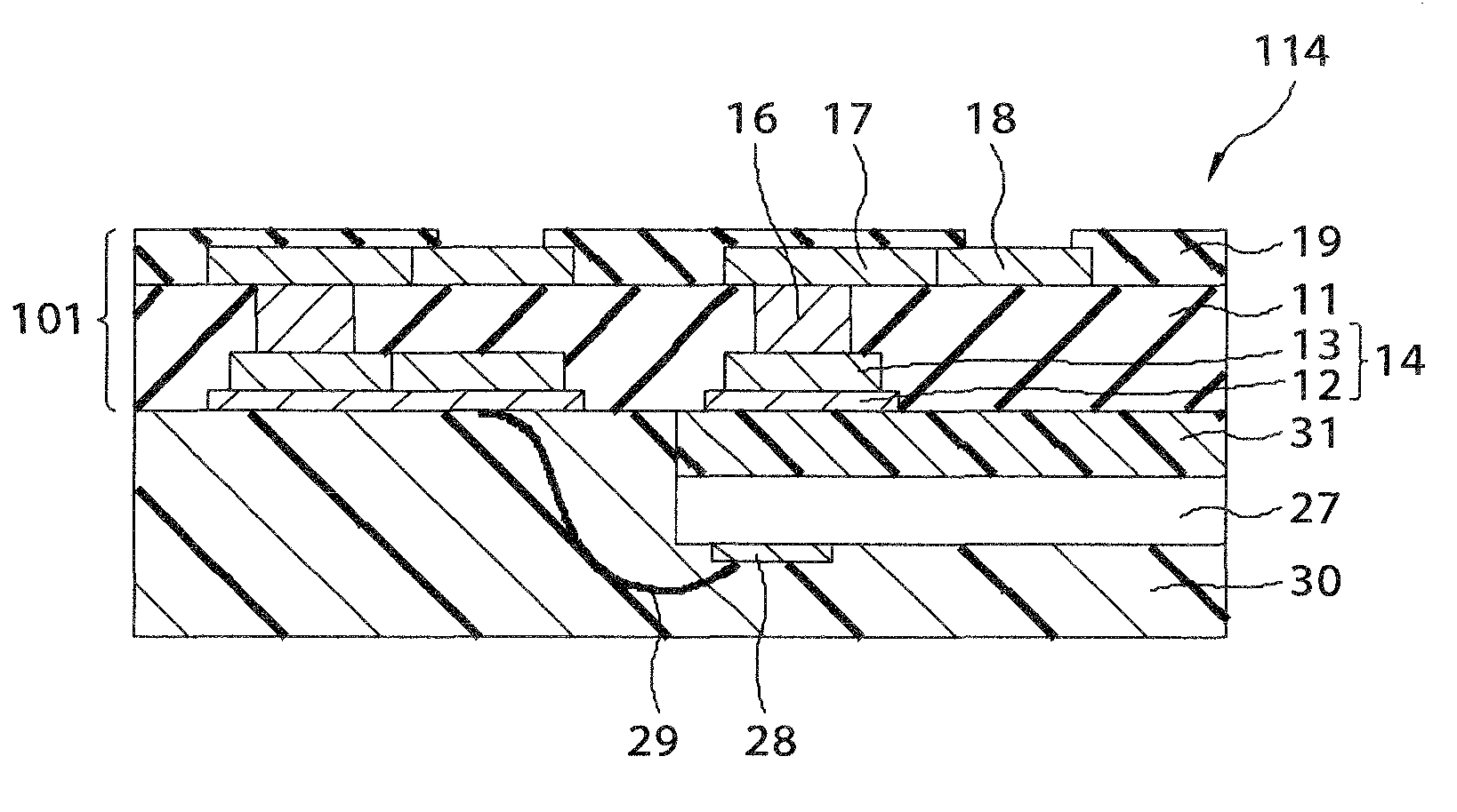
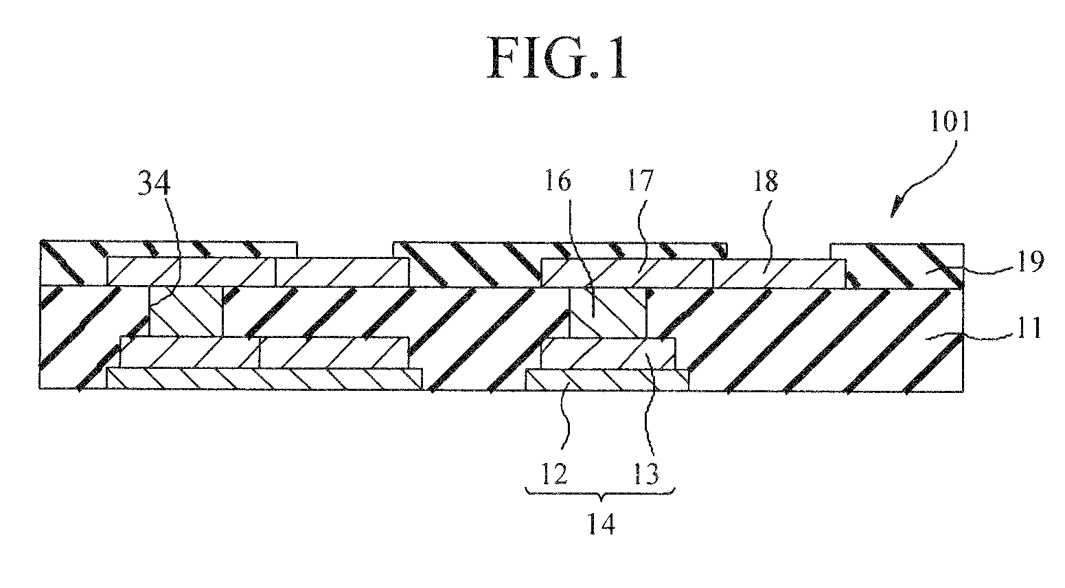
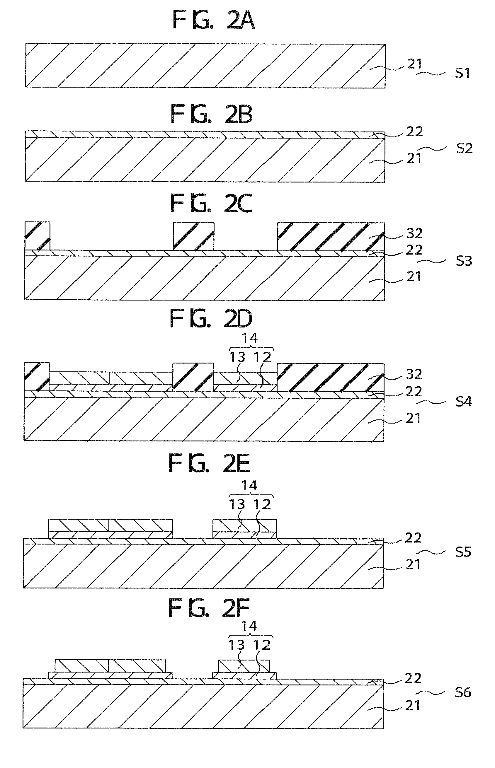
[0054]Embodiments of the present invention will be specifically explained below with reference to the attached drawings. To begin with, the present invention will be explained. FIG. 1 is an exemplary cross-sectional view of a wiring board 101 according to the present embodiment. FIGS. 2A through 2F, FIGS. 3A through 3D, and FIGS. 4A through 4C are exemplary cross-sectional views showing an example of the manufacturing method of the wiring board 101 according to the present embodiment step by step. FIGS. 5A through 5H are exemplary cross-sectional views showing another example of the manufacturing method till the step before FIG. 3A step by step. FIGS. 6A through 6F are exemplary cross-sectional views showing yet another example of the manufacturing method till the step before FIG. 3A step by step. FIGS. 7A through 7H are exemplary cross-sectional views showing still another example of the manufacturing method till the step before FIG. 3A step by step.

[0055]As shown in FIG. 1, the wi...

second embodiment

[0132]Next, the present invention will be explained. FIG. 8 is an exemplary cross-sectional view of a wiring board 102 according to the present embodiment. FIGS. 9A through 9E, FIGS. 10A through 10D and FIGS. 11A through 11C are exemplary cross-sectional views showing one example of a manufacturing method of the wiring board 102 according to the present embodiment step by step. FIGS. 12A through 12G are exemplary cross-sectional views showing another example of the manufacturing method till the step before FIG. 11A step by step. In FIG. 8 through FIG. 12, components that are the same as those in FIG. 1 through FIG. 7 will be denoted by the same reference numerals and will not be explained in detail again.

[0133]In the first embodiment described above, the first wiring layer 14 is embedded in the insulating layer 11 with its surface exposed, and the surface of the first wiring layer 14 and the lower surface of the insulating layer 11 are coplanar. The present embodiment differs from t...

third embodiment

[0181]Next, the present invention will be explained. FIG. 13 is an exemplary cross-sectional view of a wiring board 103 according to the present embodiment. FIGS. 14A through 14H are exemplary cross-sectional views showing one example of a manufacturing method of the wiring board 103 according to the present embodiment step by step. In FIG. 13 and FIG. 14, components that are the same as those in FIG. 1 through FIG. 12 will be denoted by the same reference numerals and will not be explained in detail again.

[0182]In the second embodiment described above, the side surfaces of the depression coincide with the edges of the first metal film 13. The present embodiment differs from the second embodiment in that the side surfaces of the depression 15 are located more outward than the edges of the first metal film 12, but is the same as the first embodiment in the other respects.

[0183]As shown in FIG. 13, in the wiring board 103 according to the present embodiment, the first metal film 12 is...


PUM


Abstract

A wiring board has an insulating layer, a plurality of wiring layers formed in such a way as to be insulated from each other by the insulating layer, and a plurality of vias formed in the insulating layer to connect the wiring layers. Of the wiring layers, a surface wiring layer formed in one surface of the insulating layer include a first metal film exposed from the one surface and a second metal film embedded in the insulating layer and stacked on the first metal film. Edges of the first metal film project from edges of the second metal film in the direction in which the second metal film spreads. By designing the shape of the wiring layers embedded in the insulating layer in this manner, it is possible to obtain a highly reliable wiring board that can be effectively prevented from side etching in the manufacturing process and can adapt to miniaturization and highly dense packaging of wires.

Description

TECHNICAL FIELD[0001]The present invention relates to a wiring board on which a semiconductor element is to be mounted, a semiconductor device formed of a semiconductor element mounted on the wiring board, and their manufacturing methods, and particularly to a thin wiring board excellent in high-speed transmission characteristic and mounting reliability, a semiconductor device using the wiring board, and their manufacturing methods.BACKGROUND ART[0002]As can be observed from portable devices, electronic devices are now radically advancing toward acquiring a smaller, thinner, and more densely packaged body. Further, improvement in speed and functions of semiconductor elements has increased the number of their terminals, and this requires that a wiring board used for device mounting and semiconductor element mounting should be thinner, lighter, and more suited for dense packaging.[0003]Typical wiring boards have been those that have through holes, such as built-up boards. However, suc...

Claims


Application Information

Patent Timeline
Patent Type & Authority Patents(United States)
IPC IPC(8): H01L23/495
CPCH01L21/4857H01L21/486H01L21/563H01L23/498H01L23/49822H01L23/49827H05K3/205H01L2224/48091H01L2224/48472H01L2224/73203H01L2924/01004H01L2924/01025H01L2924/01046H01L2924/01057H01L2924/01078H01L2924/01079H01L2924/09701H01L2924/12044H01L2924/19041H05K3/244H05K3/423H05K2201/0338H05K2201/098H05K2201/09845H05K2203/0376H05K2203/0384H05K2203/0733H05K2203/1476H01L2924/00014H01L24/48H01L2924/01019H01L2924/01322H01L2224/16225H01L2224/32225H01L2224/48227H01L2224/73204H01L2224/73265H01L2224/92247H01L2924/00H01L2924/00012H01L2924/181H01L2224/48228H01L24/73H01L2224/05573H01L2224/05568H01L2224/45144H01L24/45H01L2224/05599H01L2224/45015H01L2924/207
Inventor KIKUCHI, KATSUMIYAMAMICHI, SHINTAROMURAI, HIDEYAFUNAYA, TAKUOMORI, KENTAROMAEDA, TAKEHIKOHONDA, HIROKAZUOGAWA, KENTATSUKANO, JUN
Owner RENESAS ELECTRONICS CORP
Why Eureka
Try Eureka