Variable-frequency band-elimination filter

a filter and variable frequency band technology, applied in filters, multiple-port networks, electrical devices, etc., can solve the problems of deterioration of filter characteristics of variable frequency band filters, increased size of transmission/receiving modules, complex system configuration, etc., and achieve excellent filter characteristics and simple configuration.

Active Publication Date: 2011-03-22
MURATA MFG CO LTD
View PDF13 Cites 19 Cited by
  • Summary
  • Abstract
  • Description
  • Claims
  • Application Information

AI Technical Summary

Benefits of technology

[0011]To overcome the problems described above, preferred embodiments of the present invention provide a small and low-cost variable-frequency band-elimination filter which has a simple configuration and which is capable of shifting a frequency while maintaining excellent filter characteristics.
[0017]According to various preferred embodiments of the present invention, the following advantages are obtained. A plurality of series resonance circuits (LC series resonance circuits), each of which is connected in shunt with a signal line and is defined by an inductor and a capacitor, are provided, and a matching circuit is connected between two series resonance circuits adjacent to each other, such that a band-elimination filter including a plurality of resonators is obtained. Since the inductance of each of the series resonance circuits is changed by turning on or off a switching element, the number of components included in a variable-frequency band-elimination filter is reduced. This reduces the size and cost of the variable-frequency band-elimination filter. Furthermore, since a filter characteristic is changed using the switching element, it is not necessary to use a plurality of paths and a plurality of filters as described in Japanese Unexamined Patent Application Publication No. 10-289342 and Japanese Unexamined Patent Application Publication No. 9-199996. As a result, the number of elements of the filter is reduced. Still furthermore, since the inductance component of the switching element is added only to an inductor connected to the switching element when the switching element is in an ON state, it is possible to prevent the inductance component of the switching element from adversely affecting filter characteristics.
[0018]Since a matching circuit is preferably defined by a multistage T-shape circuit including inductors connected in series to one another and capacitors connected in shunt with each other, the design flexibility required to satisfy a matching condition is increased and a desired matching condition among a plurality of LC series resonance circuits can be obtained. That is, if a band elimination filter has a pass band on both sides of a variable resonance point, it is impossible to obtain a desired matching condition using a simple circuit and to obtain a sufficient band elimination characteristic when the inductance of each of series resonance circuits is changed by turning on or off a switching element. However, by using a multistage T-shape LCL circuit, it is possible to achieve matching among these series resonance circuits in a wide frequency range and to obtain a sufficient band elimination characteristic in both of the ON and OFF states of the switching element.
[0019]Since a FET (Field Effect Transistor) is preferably used as the switching element, it is possible to reduce a current that flows when the switching element is in the ON state. This results in reduced power consumption and a reduced size of a variable-frequency band-elimination filter.
[0020]Since a bias circuit arranged to apply a single control voltage to a switching element connected between each of the grounding ends of a plurality of LC series resonance circuits and the ground is provided, it is possible to control a frequency characteristic using a single power source. This results in a further reduced size of an entire circuit.
[0021]Since the switching elements, the inductors, the capacitors, and frequency shifting inductors are preferably provided on or in a multilayer substrate, it is possible to easily dispose these components on a circuit board of an electronic apparatus as a single small component.

Problems solved by technology

As a result, the size of a transmission / receiving module is increased, and a system configuration is complicated.
As a result, the filter characteristics of the variable frequency band filter are deteriorated.

Method used


Image

  • Variable-frequency band-elimination filter
  • Variable-frequency band-elimination filter
  • Variable-frequency band-elimination filter

Examples


first preferred embodiment

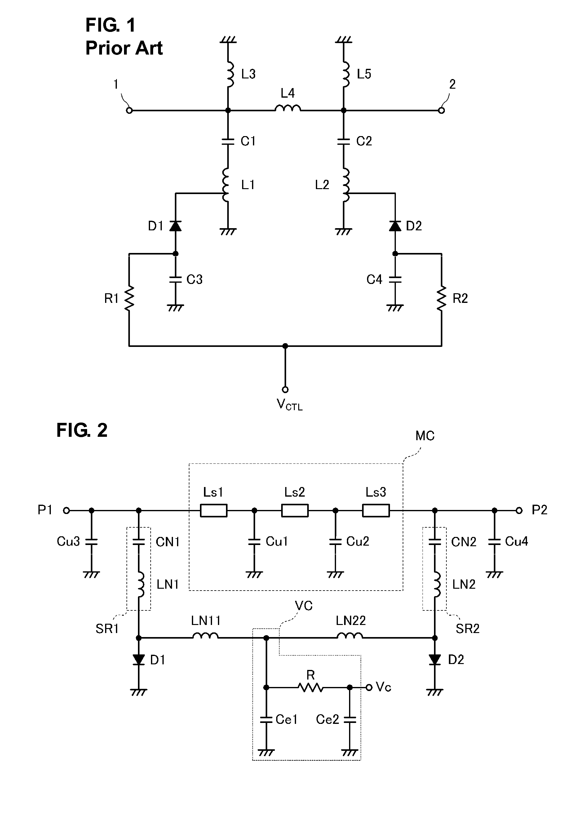
[0031]A variable-frequency band-elimination filter according to the first preferred embodiment of the present invention will be described with reference to FIGS. 2 to 5. FIG. 2 is a circuit diagram of a variable-frequency band-elimination filter according to the first preferred embodiment of the present invention.

[0032]Referring to FIG. 2, a first series resonance circuit SR1 is defined by a series circuit including an inductor LN1 and a capacitor CN1, and a second series resonance circuit SR2 is defined by a series circuit including an inductor LN2 and a capacitor CN2.

[0033]A matching circuit MC is disposed between the first series resonance circuit SR1 and the second series resonance circuit SR2. The matching circuit MC is defined by a two-stage T-shape circuit including inductors Ls1, Ls2, and Ls3 connected in series to one another and capacitors Cu1 and Cu2 connected in shunt with each other. A first-stage T-shape circuit is defined by the inductors Ls1 and Ls2 and the capacitor...

second preferred embodiment

[0050]FIG. 6 is a circuit diagram of a variable-frequency band-elimination filter according to the second preferred embodiment of the present invention. A circuit according to the second preferred embodiment illustrated in FIG. 6 differs from the circuit according to the first preferred embodiment illustrated in FIG. 2 in that each switching element is defined by a series circuit including a plurality of diodes (two diodes in this example). That is, a series circuit including two diodes D1a and D1b is disposed between the grounding end of the first series resonance circuit SR1 and the ground, and a series circuit including two diodes D2a and D2b is disposed between the grounding end of the second series resonance circuit SR2 and the ground.

[0051]Thus, by connecting a plurality of diodes in series, an equivalent capacitance component can be reduced when these diodes are in the OFF state. Furthermore, by turning on or off the diodes D1a and D1b connected in series to each other and th...

third preferred embodiment

[0052]FIG. 7 is a circuit diagram of a variable-frequency band-elimination filter according to the third preferred embodiment of the present invention. In this example, a FET is preferably used as a switching element. That is, a FET Q1 is disposed between the grounding end of the first series resonance circuit SR1 and the ground, and a FET Q2 is disposed between the grounding end of the second series resonance circuit SR2 and the ground. The connection point between the grounding end of the first series resonance circuit SR1 and the FET Q1 is connected to the ground via the frequency shifting inductor LN11, and the connection point between the grounding end of the second series resonance circuit SR2 and the FET Q2 is connected to the ground via the frequency shifting inductor LN22.

[0053]A bias circuit including the capacitors Ce1 and Ce2 and the resistor R is disposed for the gates of the FETs Q1 and Q2.

[0054]In FIG. 7, if the FETs Q1 and Q2 are N-channel FETs and a predetermined po...


PUM


Abstract

A series resonance circuit defined by a series circuit including an inductor and a capacitor and a series resonance circuit defined by a series circuit including an inductor and a capacitor are connected in shunt to a signal line. A diode is disposed between the grounding end of the series resonance circuit and the ground, and a diode is disposed between the grounding end of the series resonance circuit and the ground. The connection point between the grounding end of the series resonance circuit and the diode is connected to the ground via a frequency shifting inductor in a conductive state at high frequency, and the connection point between the grounding end of the series resonance circuit and the diode is connected to the ground via a frequency shifting inductor in a conductive state at high frequency. A matching circuit defined by a multistage T-shape LCL circuit is disposed between the series resonance circuits.

Description

BACKGROUND OF THE INVENTION[0001]1. Field of the Invention[0002]The present invention relates to variable-frequency filters, and more particularly, to a variable-frequency band-elimination filter for changing a frequency band using a switching element.[0003]2. Description of the Related Art[0004]Japanese Unexamined Patent Application Publication No. 10-289342 discloses a communication system in which switching between a plurality of filters having pass bands corresponding to different frequency bands is performed using switches.[0005]That is, a switch is disposed at the input ends of two signal paths passing through filters having different filter characteristics, another switch is disposed at the output ends of the two signal paths, and switching between the filter characteristics is performed by operating each of these switches.[0006]Japanese Unexamined Patent Application Publication No. 7-321586 discloses a filter in which filters having different characteristics are individually...

Claims


Application Information

Patent Timeline
Patent Type & Authority Patents(United States)
IPC IPC(8): H03H7/01
CPCH03H7/0115H03H7/0153H03H7/1758H03H7/1775H03H7/1791H03H2007/013H03H2210/012
Inventor HARADA, TETSUROTONEGAWA, KEN
Owner MURATA MFG CO LTD
Why Eureka
Try Eureka