

Semiconductor device and manufacturing of the same
a semiconductor device and manufacturing method technology, applied in the direction of semiconductor devices, electrical devices, transistors, etc., can solve the problem of not being able to achieve the leakage current level required in the roadmap, and achieve the effect of improving the performance of the semiconductor device, increasing the leakage current, and reducing the mobility of the carrier
- Summary
- Abstract
- Description
- Claims
- Application Information
AI Technical Summary
Benefits of technology
Problems solved by technology
Method used
Image

Examples
first embodiment
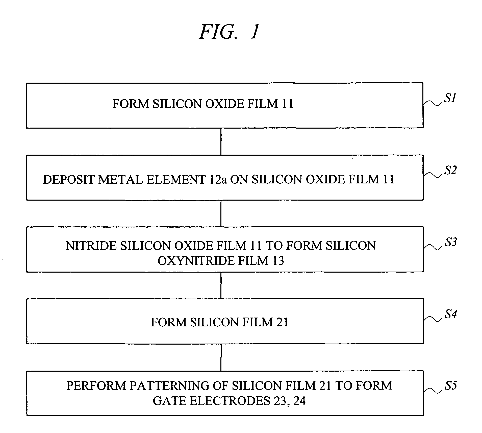
[0070]The semiconductor device and the manufacturing method of the semiconductor device according to the first embodiment will be described with reference to the drawings.
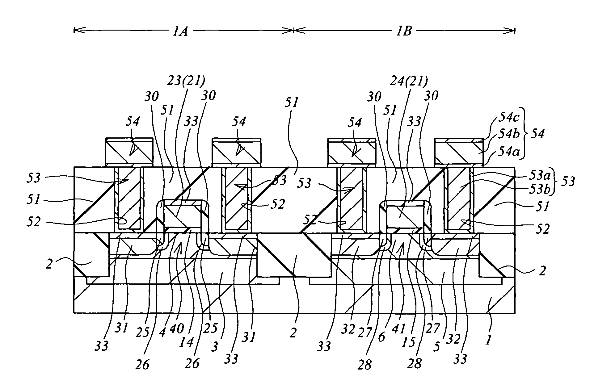
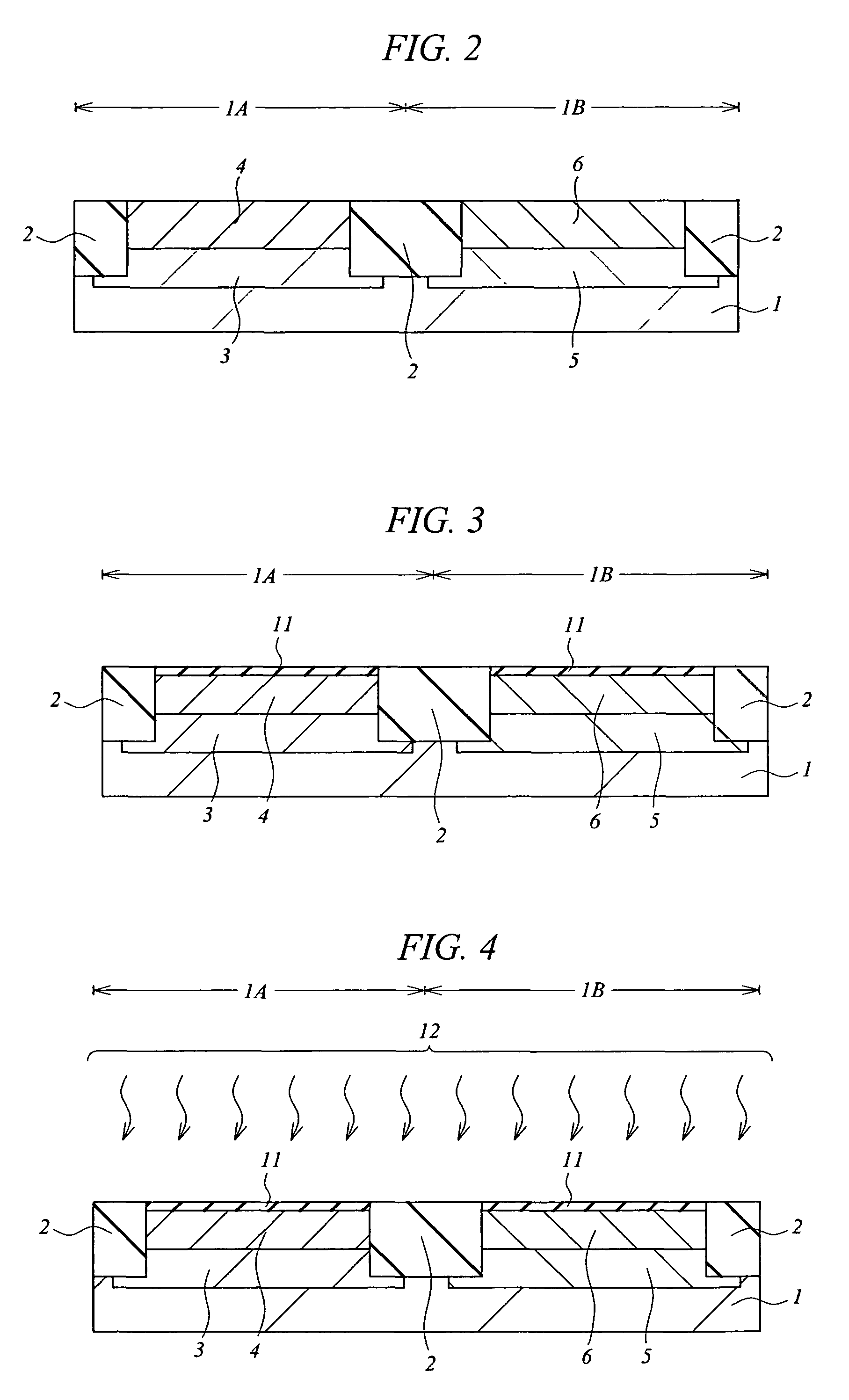
[0071]FIG. 1 is a process flowchart showing a manufacturing process of a semiconductor device according to the present embodiment. FIG. 2 to FIG. 4, FIG. 6, FIG. 7, and FIG. 9 to FIG. 12 are cross-sectional views of main parts in the manufacturing process of a semiconductor device according to the present embodiment. FIG. 5 is a partially-enlarged cross-sectional view (cross-sectional view of the main parts) schematically showing the state where a minute amount of metal elements 12a is deposited on a silicon oxide film 11. FIG. 8 is a partially-enlarged cross-sectional view (cross-sectional view of the main parts) schematically showing the state where a silicon film 21 is formed on a silicon oxynitride film 13. Note that a process from a step of forming an insulating film (silicon oxide film 11) for forming a gate ...
second embodiment
[0143]In the present embodiment, multi-level gate insulating. films having various (two or more types of) film thicknesses are formed on the same semiconductor substrate 1, and metal elements 12a having a surface density of 1×10¹³ to 5×10¹⁴ atoms / cm2 are introduced into the gate insulating film and the interface between the gate insulating film and the Si gate electrode. Also, the surface density of the metal elements 12a is equal in all of the gate insulating films.
[0144]FIG. 17 to FIG. 22 are cross-sectional views of main parts during a manufacturing process of a semiconductor device according to the present embodiment.
[0145]In the present embodiment, the case where two types of CMISFET 60a and 60b, one having an EOT of 1.8 nm of the gate insulating film after completion and the other having an EOT of 7.0 nm of the gate insulating film after completion, are formed will be described as an example.
[0146]As shown in FIG. 17, a semiconductor substrate (semiconductor wafer or single-cr...
third embodiment
[0178]In the present embodiment, a manufacturing method of a semiconductor device will be described, in which two types of CMISFETs having approximately equal gate insulating film thickness and different threshold voltages are formed on the same semiconductor substrate 1, and the threshold voltages are adjusted based on the amount of metal introduced into the interfaces between gate insulating films and Si gate electrodes. Note that the case where a total of three types of CMISFETs 61, 62, and 63, that is, the CMISFETs 61 and 62 in which a thickness of the gate insulating film is 1.8 nm, a power supply voltage is 1.2 V, and their absolute values of the threshold voltages are adjusted to 0.25 V and 0.5 V respectively, and the CMISFET 63 in which a gate insulating film thickness is 7.0 nm and a power supply voltage is 3.3 V are simultaneously formed will be described here as an example.
[0179]FIG. 23 to FIG. 29 are cross-sectional views of main parts during a manufacturing process of a...
PUM
 Abstract
Description
Claims
Application Information