Techniques for simultaneously driving a plurality of source lines

a technology of source line and source line, applied in the direction of information storage, static storage, digital storage, etc., can solve the problems of memory cell disruption, large power consumption, and over-the-top charge carrier

Active Publication Date: 2011-04-12
MICRON TECH INC
View PDF381 Cites 121 Cited by
  • Summary
  • Abstract
  • Description
  • Claims
  • Application Information

AI Technical Summary

Problems solved by technology

Also, conventional writing techniques for memory cells having an N-Channel type memory transistor typically result in an excess of majority charge carriers by channel impact ionization or by band-to-band tunneling (gate-induced drain leakage “GIDL”).
Often, conventional reading and writing techniques may lead to relatively large power consumption and large voltage drivers which occupy large amount of area on a circuit board or die and cause disruptions to memory cells on unselected rows of an array of memory cells.
However, some of the minority charge carriers may remain “trapped” in interface defects.
This phenomenon may be characterized as charge pumping, which is a problem because the net quantity of charge carriers may be reduced in an electrically floating body region of the memory cell, which, in turn, may gradually reduce, and even eliminate, a net charge representing data stored in the memory cell.
In view of the foregoing, it may be understood that there are significant problems and shortcomings associated with reading from and / or writing to electrically floating body semiconductor dynamic random access memory (“DRAM”) devices using conventional reading / writing techniques.

Method used


Image

  • Techniques for simultaneously driving a plurality of source lines
  • Techniques for simultaneously driving a plurality of source lines
  • Techniques for simultaneously driving a plurality of source lines

Examples


Embodiment Construction

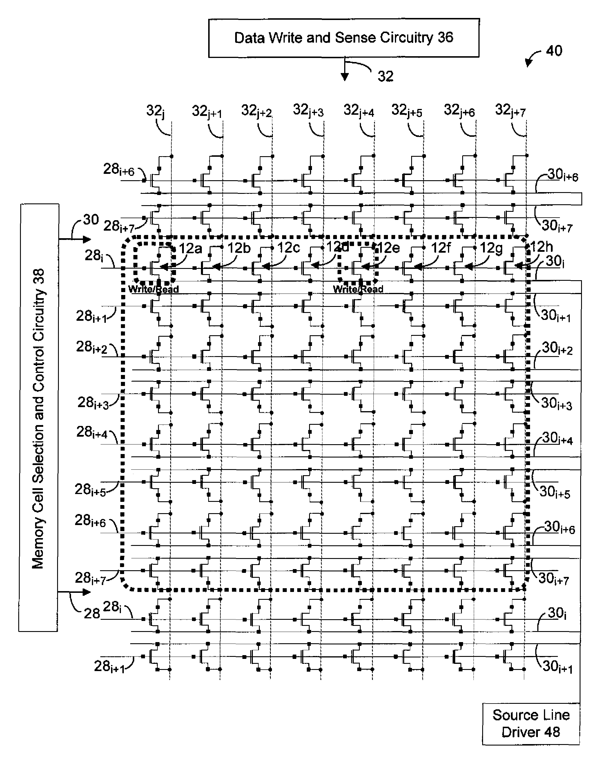
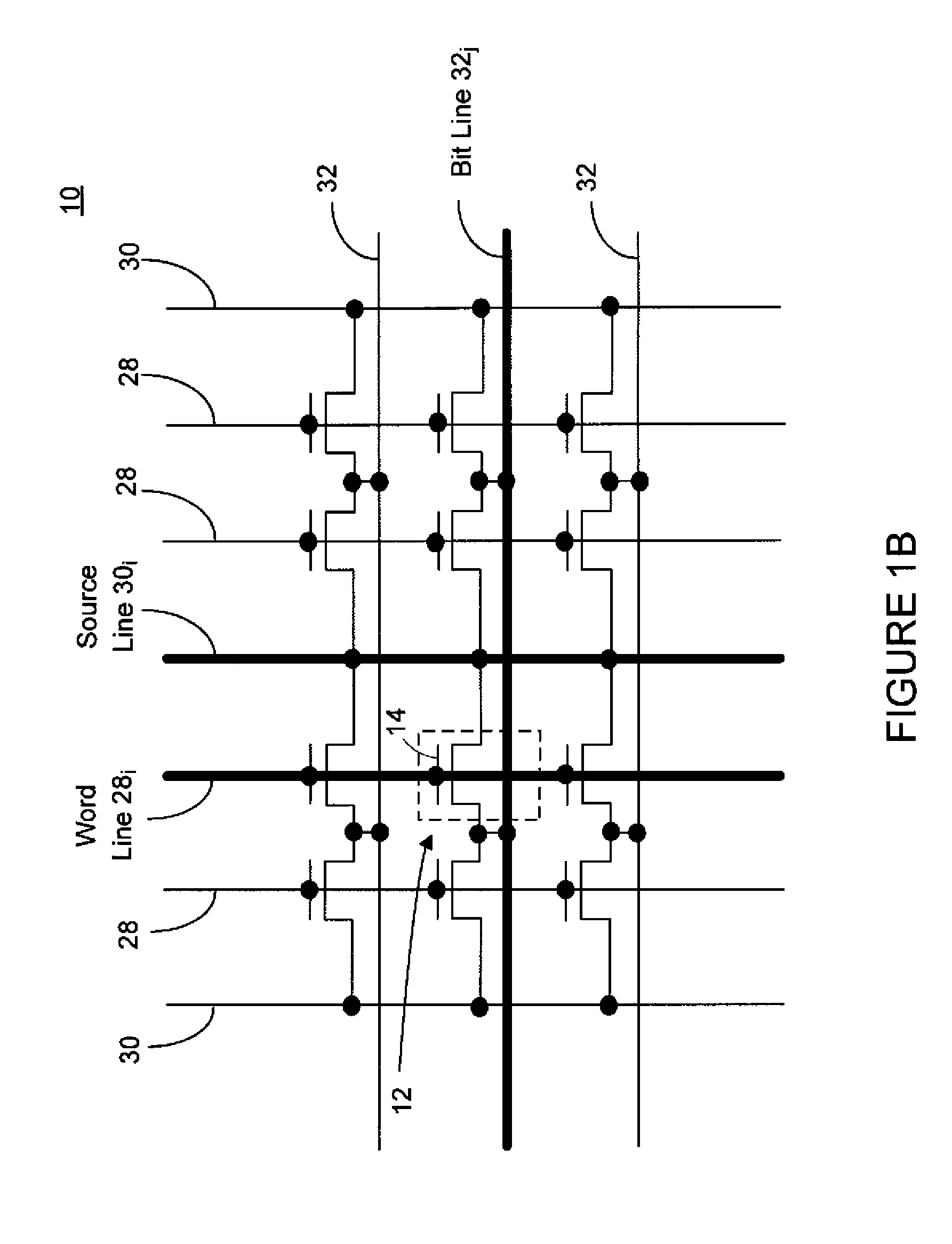
[0041]There are many embodiments described and illustrated herein. In one aspect, the present disclosure is directed to a combination of reading / writing methods which comprise simultaneously driving a plurality of source lines (SL). Also, the present disclosure is directed to providing a relatively high voltage when reading from and / or writing to memory cells so as to reduce disruptions to unselected memory cells and increase retention time.

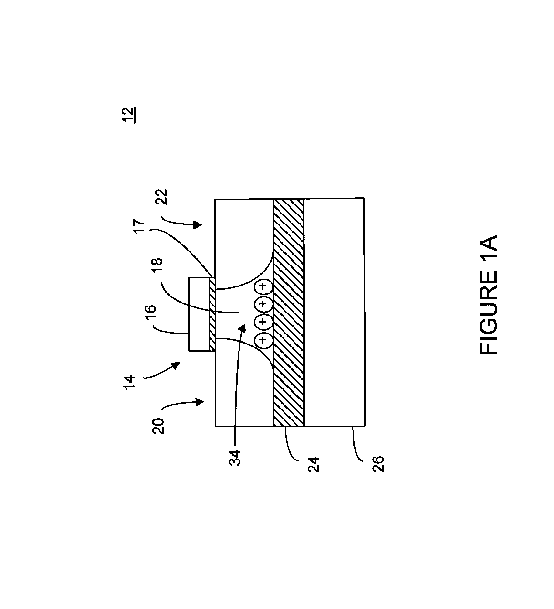
[0042]Referring to FIG. 1A, there is a shown a cross-sectional view of a memory cell 12 in accordance with an embodiment of the present disclosure. The memory cell 12 may comprise a memory transistor 14 (e.g., an N-channel type transistor or a P-channel type transistor) including a source region 20, a drain region 22, and an electrically floating body region 18 disposed between the source region 20 and the drain region 22. Charge carriers 34 may be accumulated in or may be emitted / ejected from the electrically floating body region 18. A data stat...


PUM


Abstract

Techniques for simultaneously driving a plurality of source lines are disclosed. In one particular exemplary embodiment, the techniques may be realized as an apparatus for simultaneously driving a plurality of source lines. The apparatus may include a plurality of source lines coupled to a single source line driver. The apparatus may also include a plurality of dynamic random access memory cells arranged in an array of rows and columns, each dynamic random access memory cell including one or more memory transistors. Each of the one or more memory transistors may include a first region coupled to a first source line of the plurality of source lines, a second region coupled to a bit line, a body region disposed between the first region and the second region, wherein the body region may be electrically floating, and a gate coupled to a word line and spaced apart from, and capacitively coupled to, the body region.

Description

FIELD OF THE DISCLOSURE[0001]The present disclosure relates generally to semiconductor dynamic random access memory (“DRAM”) devices and, more particularly, to techniques for simultaneously driving a plurality of source lines (SL) in a semiconductor dynamic random access memory (“DRAM”) device.BACKGROUND OF THE DISCLOSURE[0002]There is a continuing trend to employ and / or fabricate advanced integrated circuits using techniques, materials, and devices that improve performance, reduce leakage current, and enhance overall scaling. Semiconductor-on-insulator (SOI) is a material which may be used to fabricate such integrated circuits. Such integrated circuits are known as SOI devices and may include, for example, partially depleted (PD) devices, fully depleted (FD) devices, multiple gate devices (for example, double or triple gate), and Fin-FET devices.[0003]One example of an SOI device is a semiconductor dynamic random access memory (“DRAM”) device. Such a semiconductor DRAM device may i...

Claims


Application Information

Patent Timeline
Patent Type & Authority Patents(United States)
IPC IPC(8): G11C7/10G11C5/06G11C7/00G11C8/00
CPCG11C11/404G11C11/4074G11C11/4094G11C11/4076G11C2211/4016G11C11/406
Inventor CARMAN, ERIC
Owner MICRON TECH INC
Why Eureka
Try Eureka