Method for manufacturing image display device

a technology of image display and manufacturing method, which is applied in the direction of identification means, instruments, electric/magnetic/electromagnetic heating, etc., can solve the problems of display defects, deformation of optical glass, and gap 105 as an obstacle to the reduction of panel thickness, so as to prevent the irregular orientation of liquid crystal material, the effect of reducing the influence of stress

Active Publication Date: 2011-04-19
DEXERIALS CORP
View PDF44 Cites 40 Cited by
  • Summary
  • Abstract
  • Description
  • Claims
  • Application Information

AI Technical Summary

Benefits of technology

[0017]The internal stress accumulated during curing of the resin can be approximated by the product of the storage elastic modulus after curing and the curing shrinkage ratio. In the present invention, the curable resin composition used has a curing shrinkage ratio of 5% or less and yields a cured product having a storage elastic modulus at 25° C. of 1.0×10⁷ Pa or less. The use of such a curable resin composition provides a suitable relationship between the elastic modulus and curing shrinkage ratio of the resin filling the gap between the image display unit and the protection member, and can minimize the influence of the stress during curing and shrinkage of the resin on the image display unit and the protection member. Therefore, almost no strain occurs in the image display unit and the protection member. Accordingly, a high-brightness and high-contrast image can be displayed without display defects.
[0018]In particular, when the image display unit is a liquid crystal display panel, display defects such as irregularities in orientation of the liquid crystal material can be reliably prevented, so that a high quality image can be displayed.
[0019]In the present invention, the cured resin is interposed between the image display unit and the protection member, and this provides high impact resistance.
[0020]Moreover, an image display device thinner than that in the conventional example in which a gap is formed between the image display unit and the protection member can be provided.
[0021]In addition, in the present invention, a photo-curable resin composition is used as the curable resin composition interposed between the image display unit and the protection member, and is irradiated with rays of light at least from an outer side surface with respect to a forming surface of the light-shielding member. Therefore, the photo-curable resin composition in the area where the light-shielding member is formed is properly irradiated with rays of light and cured sufficiently.

Problems solved by technology

The presence of the gap 105 is an obstacle to the reduction in thickness of the panel.
However, the stress during the cure shrinkage of the cured resin causes deformation of the optical glass plates sandwiching the liquid crystal of the liquid crystal display panel.
This results in display defects such as irregularities in orientation of the liquid crystal material.
However, in such a structure, when the gap 105 between the liquid crystal display panel 102 and the protection member 103 is filled with a photo-curable resin composition and rays of light is irradiated to cure the resin composition, the resin composition present in an area where the light-shielding member is formed may not be cured.

Method used


Image

  • Method for manufacturing image display device
  • Method for manufacturing image display device
  • Method for manufacturing image display device

Examples


experimental example 1

[0076]The resin compositions of Examples 1 to 4 and the resin compositions of Comparative Examples 1 to 3 were applied dropwise to 100 μm-thick white glass plates so as to have a predetermined thickness. The glass plates were carried into a UV conveyer, whereby the cured products of the resins having a predetermined thickness were obtained and used as samples.

[0077]Each of the samples was measured for “light transmittance”, “storage elastic modulus”, “curing shrinkage ratio”, and “surface roughness” as follows. The results are shown in Table 1.

[Light Transmittance]

[0078]The light transmittance (%) in the visible range was measured for each sample (the thickness of the cured resin: 100 μm) using an ultraviolet and visible spectrophotometer (V-560, product of JASCO Corporation) and was found to be 90% or more for all the samples.

[Storage Elastic Modulus]

[0079]The storage elastic modulus (Pa, 25° C.) was measured for each sample at a measurement frequency of 1 Hz using a viscoelasticit...

experimental example 2

Measurement of Cure Ratio

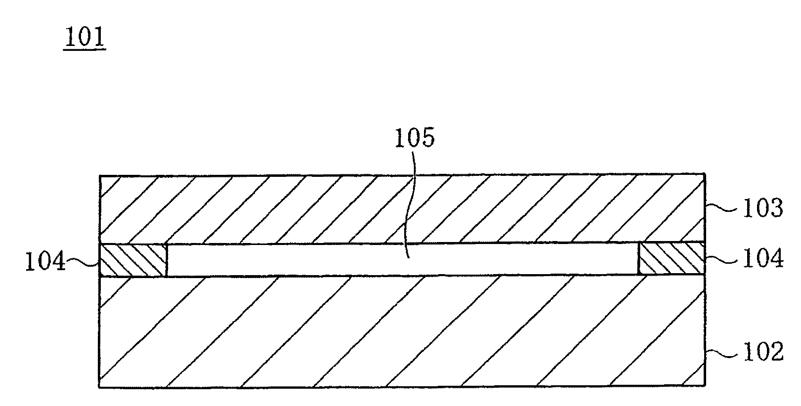
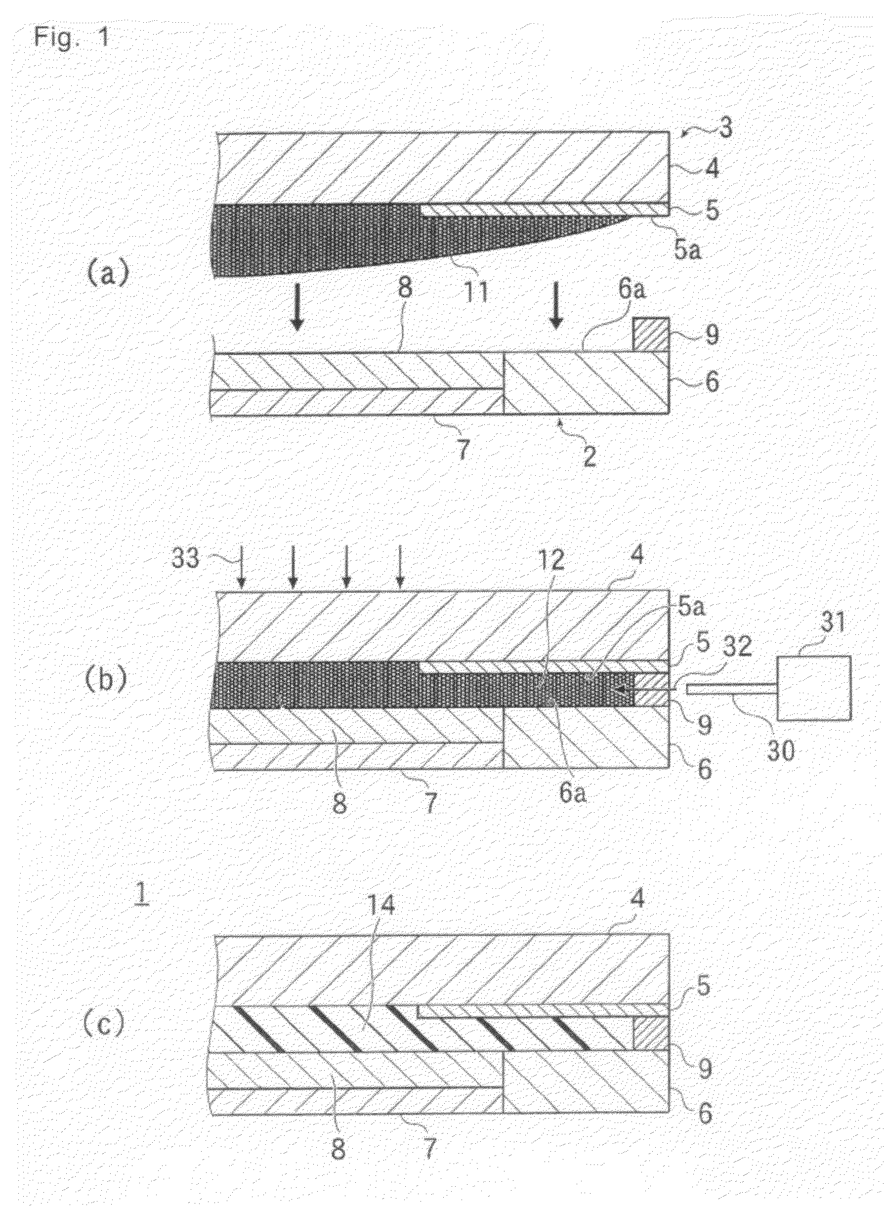
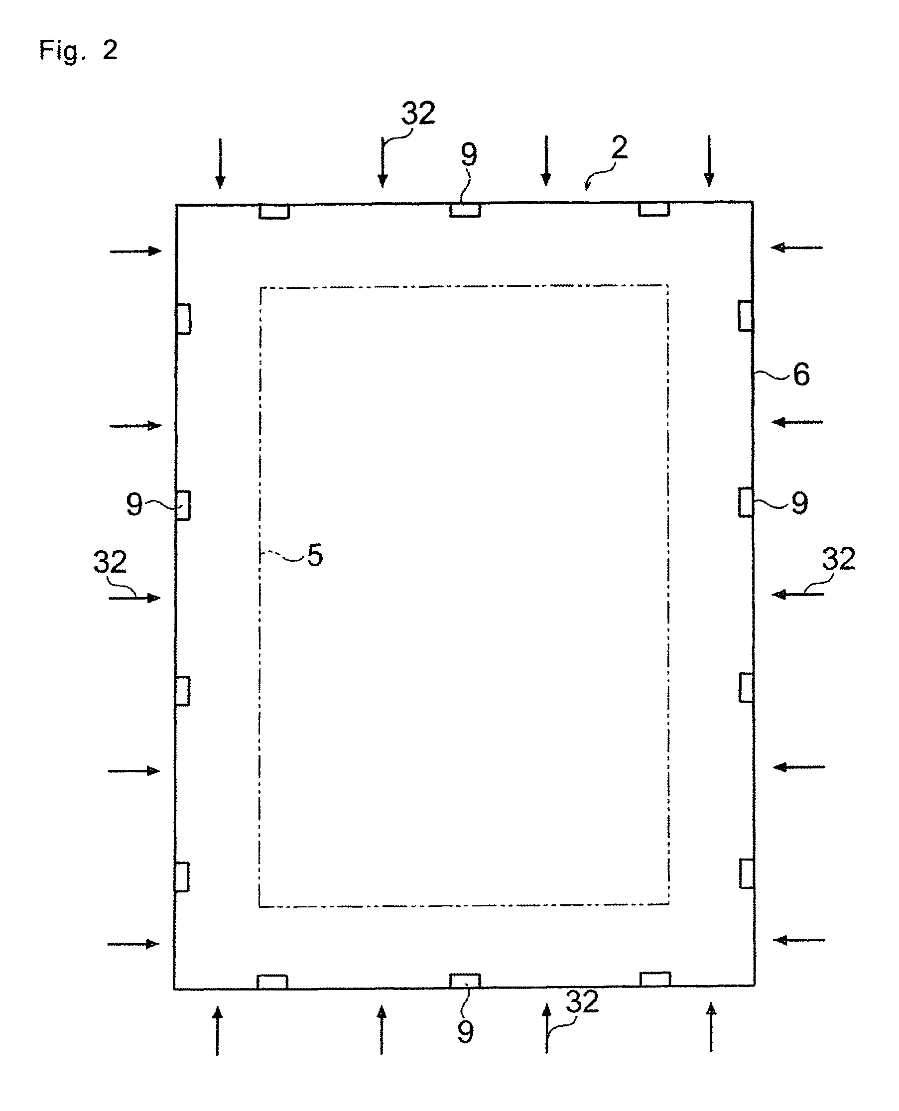
[0084]About 0.2 g of the resin composition of Example 1 prepared in Experimental Example 1 was applied dropwise to an acrylic plate to be used as the protection member 3 in FIG. 1(a). The acrylic plate was disposed on a liquid crystal display panel to be used as the base 2 so as to face each other, whereby the gap between the liquid crystal panel and the acrylic plate was filled with the resin composition of Example 1. Three sets of such samples were prepared. In two of the samples used, a light-shielding member (black matrix) 5 composed of a 2 mm-width black ink layer was formed on the peripheral area of the acrylic plate. In the remaining one of the samples used, the light-shielding member 5 was not formed.

[0085]One sample including the acrylic plate having the light-shielding member 5 formed thereon was irradiated with UV rays (front irradiation) at an integrated light intensity of 5,000 mJ using a UV lamp (product of USHIO Inc.) placed about 10 cm away f...


PUM

PropertyMeasurementUnit
light transmittanceaaaaaaaaaa
storage elastic modulusaaaaaaaaaa
curing shrinkage ratioaaaaaaaaaa

Abstract

A thin image display device having a resin interposed between an image display unit and a protection member having a light-shielding member is manufactured. In the manufactured image display device, display defects caused by the deformation of the image display unit do not occur, and high-brightness and high-contrast display can be achieved. In addition, the resin in the area where the light-shielding member is formed can be sufficiently cured. The method for manufacturing an image display device includes the step of forming a cured resin layer by interposing a photo-curable resin composition between a base including the image display unit and a light-transmitting protection member including a light-shielding member and then photo-curing the photo-curable resin composition. In this method, a resin composition having a curing shrinkage ratio of 5% or less, yielding a cured product having a storage elastic modulus at 25° C. of 1.0×10⁷ Pa or less, and forming the cured resin layer having a light transmittance of 90% or more in a visible range is used as the photo-curable resin composition. The photo-curable resin composition is photo-cured by irradiating it with rays of light at least from an outer side surface with respect to a forming surface of the light-shielding member.

Description

TECHNICAL FIELD[0001]The present invention relates to a method for manufacturing an image display device such as a liquid crystal display (LCD) device used, for example, in a cellular phone, and in particular, to a method for manufacturing an image display device having a transparent protection member disposed on an image display unit.BACKGROUND TECHNOLOGY[0002]One conventional example of such an image display device is one shown in FIG. 4.[0003]This liquid crystal display device 101 includes a transparent protection member 103 made of, for example, glass or plastic and disposed on a liquid crystal display panel 102.[0004]In this device, to protect the surface of the liquid crystal display panel 102 and a polarizing plate (not shown), a spacer 104 is interposed between the liquid crystal display panel 102 and the protection member 103, so that a gap 105 is provided between the liquid crystal display panel 102 and the protection member 103.[0005]However, the gap 105 present between t...

Claims


Application Information

Patent Timeline
Patent Type & Authority Patents(United States)
IPC IPC(8): B29C65/00
CPCG02F1/133308G02F1/1333G02F1/1335G02F1/133512G02F2202/28G02F2001/133331G02F2201/50G02F2202/023G02F2001/133311G02F1/133311G02F1/133331G02F1/1339G09F9/00
Inventor KAMIYA, KENJISHINYA, YOSHIHISAKAMATA, YUSUKE
Owner DEXERIALS CORP
Why Eureka
Try Eureka