Semiconductor memory device

a memory device and semiconductor technology, applied in the field of semiconductor memory devices, can solve the problems of not being applicable to a single-ended sense amplifier including a single mos transistor,

Inactive Publication Date: 2011-04-26
LONGITUDE LICENSING LTD
View PDF12 Cites 12 Cited by
  • Summary
  • Abstract
  • Description
  • Claims
  • Application Information

AI Technical Summary

Benefits of technology

[0028](1) The hierarchical sense amplifier (i.e. the local sense amplifier and global sense amplifier) is designed to cancel out temperature-dependent variations of the threshold voltage of the field effect transistor serving as the single-ended sense amplifier and shifting of the threshold voltage due to dispersions of manufacturing processes, thus improving operation margins and stabilizing sense amplification.
[0029](2) It is possible to increase the permissible range of threshold-voltage variations of field effect transistors included in a semiconductor chip; hence, it is possible to improve manufacturing yields with respect to large-scale DRAM using numerous sense amplifiers, thus reducing the manufacturing cost.
[0030](3) Due to the monitoring of the temperature dependency of the field effect transistor, it is possible to cancel out and precisely compensate for temperature-dependent variations of the threshold voltage of the field effect transistor. Due to the broadened permissible range of threshold-voltage variations of field effect transistors included in a semiconductor chip, it is possible to manufacture highly-integrated and refined semiconductor memory devices with ease.

Problems solved by technology

This technology aims at adjusting the gain of the differential amplifier circuit and is not applicable to a single-ended sense amplifier including a single MOS transistor.
Patent Document 2 fails to teach the specific circuit configuration regarding the temperature sensor, temperature compensation circuit, and the sense amplifier; hence, it is not applicable to a single-ended sense amplifier including a single MOS transistor.
This technology is preferably applicable to a bipolar sense amplifier but is not applicable to a single-ended sense amplifier including a single MOS transistor.
This technology is designed to compensate for the temperature dependency of the memory resistor but is not designed to compensate for the temperature dependency of the sense amplifier; hence, it is not applicable to a single-ended sense amplifier including a single MOS transistor.
However, these technologies are incapable of compensating for threshold-voltage variations of a single-ended sense amplifier.
Both technologies are incapable of compensating for threshold-voltage variations of a single-ended sense amplifier.

Method used


Image

  • Semiconductor memory device
  • Semiconductor memory device
  • Semiconductor memory device

Examples


Embodiment Construction

[0046]The present invention will be now described herein with reference to illustrative embodiments. Those skilled in the art will recognize that many alternative embodiments can be accomplished using the teachings of the present invention and that the invention is not limited to the embodiments illustrated for explanatory purposes.

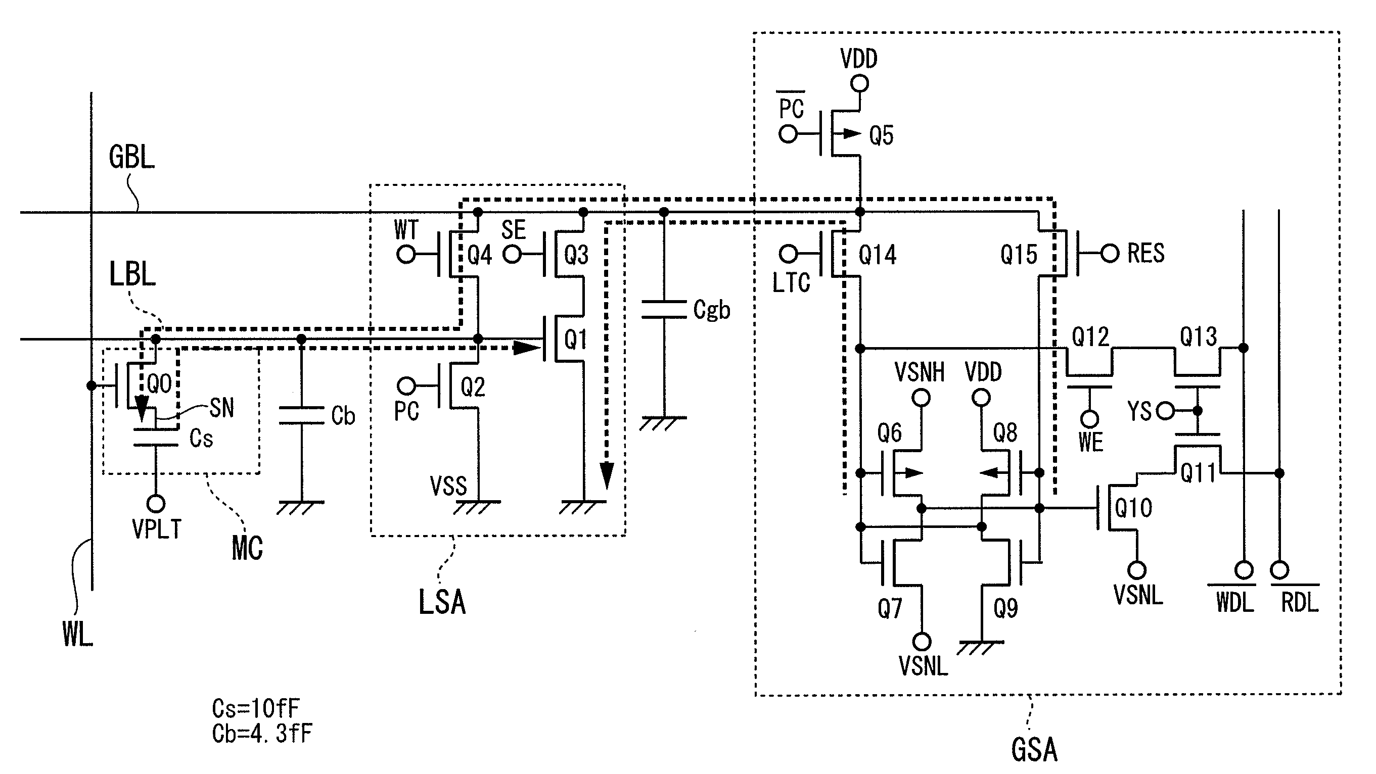
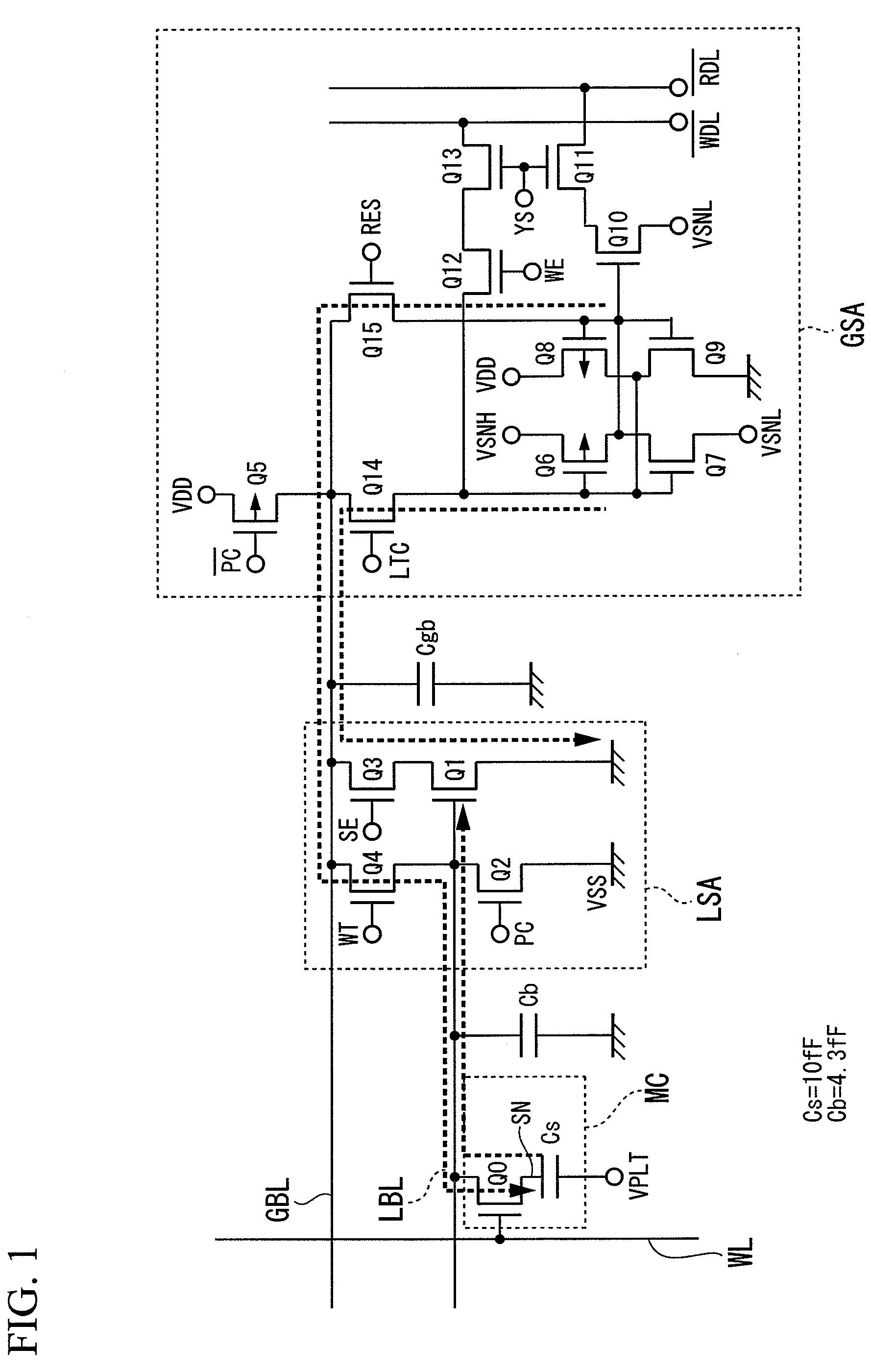
[0047]The present embodiment is directed to a single-ended sense amplifier including a MOS transistor whose gate receives a read signal voltage output onto a bit line, whose source is connected to a reference voltage such as a ground potential, and whose drain current is used to determine whether the read signal is set to “0” or “1”.

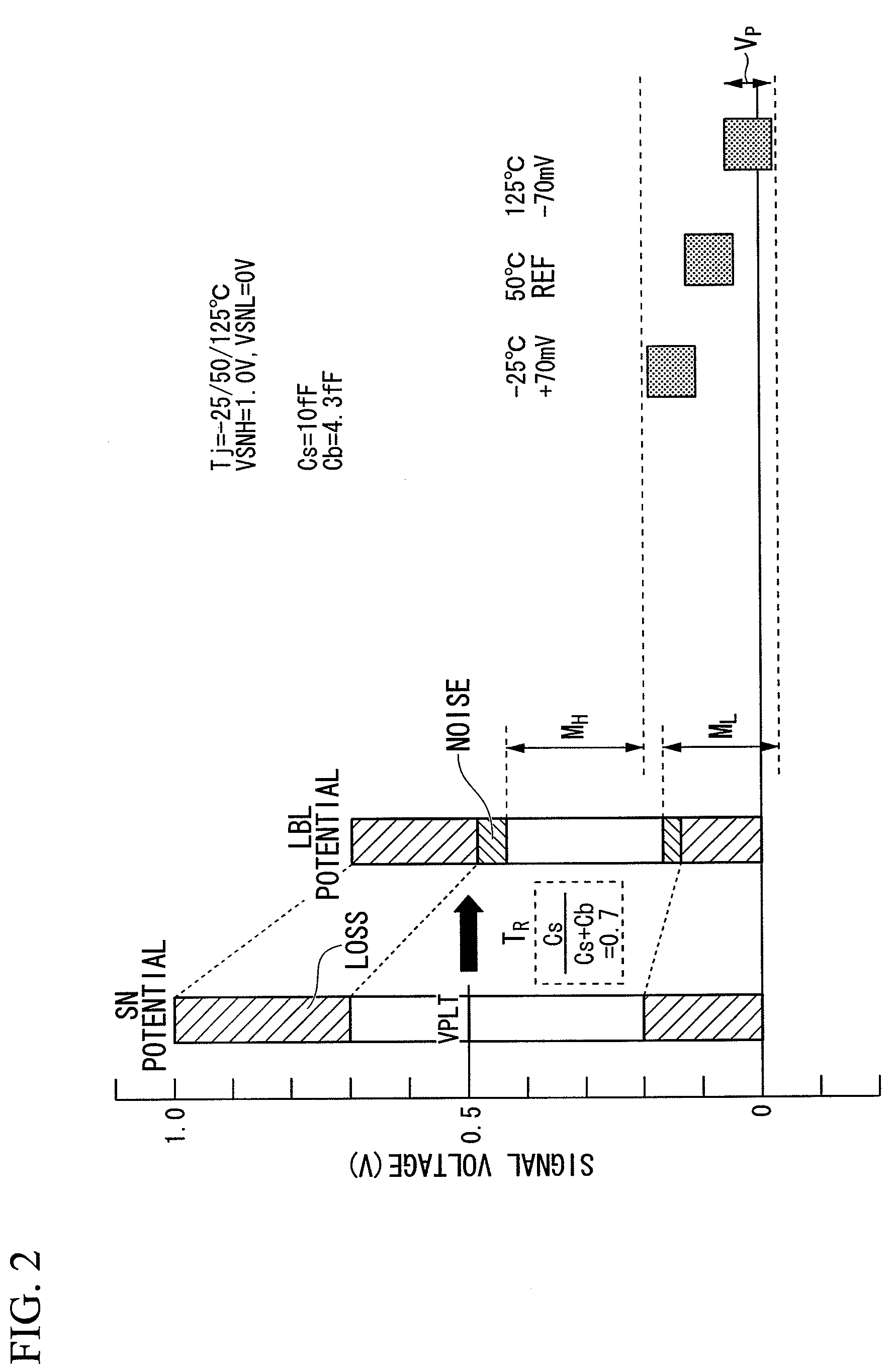
[0048]Specifically, the present embodiment is directed to the direct sensing technology adapted to a single-ended sense amplifier which inputs and amplifies a single signal. Compared to single-ended sense amplifiers, generally-known differential sense amplifiers have high gains and high noise resistance. Such high gains of dif...


PUM


Abstract

In a semiconductor memory device, a memory cell is connected with a local sense amplifier and a global sense amplifier via a local bit line and a global bit line. The local sense amplifier is a single-ended sense amplifier including a single MOS transistor, which detects a potential of the local bit line which varies when reading and writing data with the memory cell. The threshold voltage of the MOS transistor is monitored so as to produce a high-level write voltage and a low-level write voltage, which are corrected and shifted based on the monitoring result so as to properly perform a reload operation on the memory cell by the global local sense amplifier. Thus, it is possible to cancel out temperature-dependent variations of the threshold voltage and shifting of the threshold voltage due to dispersions of manufacturing processes.

Description

BACKGROUND OF THE INVENTION[0001]1. Field of the Invention[0002]The present invention relates to semiconductor memory devices such as dynamic random-access memories (DRAM), which are designed to cancel out characteristic dispersions of single-ended sense amplifiers each including a single metal-oxide semiconductor (MOS) transistor due to dispersions of threshold voltages of MOS transistors in manufacturing processes and due to temperature dependency thereof.[0003]The present application claims priority on Japanese Patent Application No. 2008-98246, the content of which is incorporated herein by reference.[0004]2. Description of Related Art[0005]Conventionally, semiconductor memory devices having sense amplifiers compensating for characteristic dispersions due to temperature variations have been developed and disclosed in various documents such as Patent Documents 1-9.[0006]Patent Document 1: Japanese Unexamined Patent Application Publication No. S58-168310[0007]Patent Document 2: Ja...

Claims


Application Information

Patent Timeline
Patent Type & Authority Patents(United States)
IPC IPC(8): G11C11/24
CPCG11C5/147G11C7/04G11C11/4097G11C11/4091G11C11/4076G11C7/06G11C7/08
Inventor KAJIGAYA, KAZUHIKOYOSHIDA, SOICHIROSEKIGUCHI, TOMONORITAKEMURA, RIICHIROYAMADA, YASUTOSHI
Owner LONGITUDE LICENSING LTD
Why Eureka
Try Eureka