Method for producing a non-planar microelectronic component using a cavity
- Summary
- Abstract
- Description
- Claims
- Application Information
AI Technical Summary
Benefits of technology
Problems solved by technology
Method used
Image

Examples
Embodiment Construction
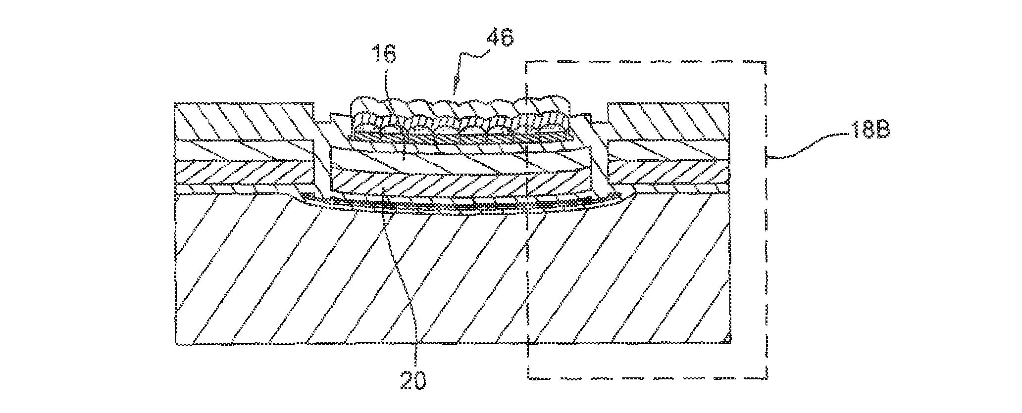
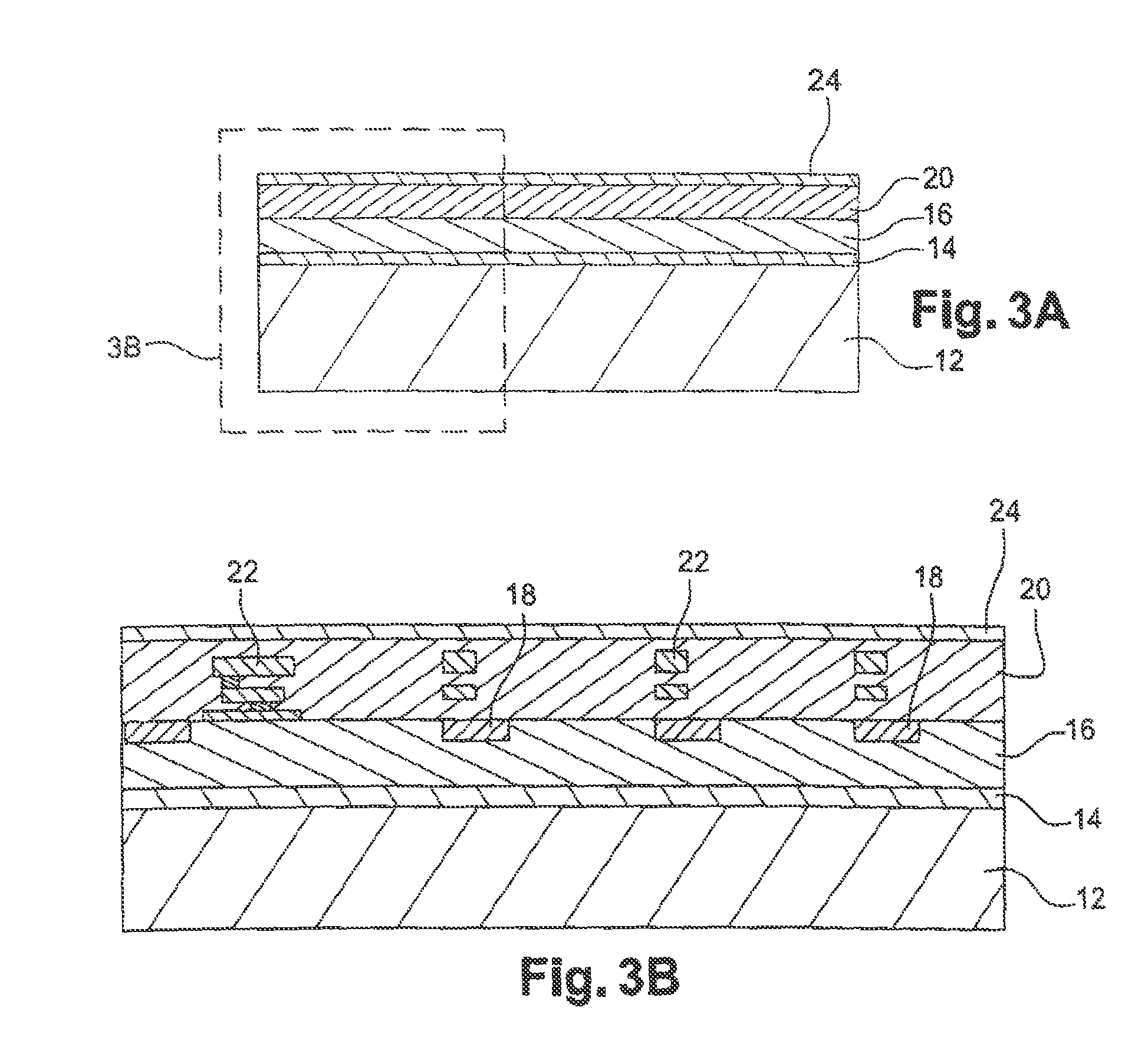
[0038]A method for fabricating a back-side electronic imager having a concave image sensor is described below.
[0039]The method starts (FIGS. 3A and 3B) by forming a thick silicon substrate 12 on which a layer of SiO2 14 having a thickness of 0.05 to 1 micrometer is deposited. Layer 14 will ultimately be used as a barrier layer when substrate 12 is thinned, as explained below in greater detail.
[0040]A silicon detection circuit 16 having a thickness of 2 to 5 μm is formed on layer 14 and comprises unitary detection elements 18 (phototransistors or photodiodes for example), or “pixels”, as well as the imager's electronic analogue and logic processing components. This therefore constitutes the active circuit in the sense of the invention.
[0041]Metallic interconnections 22 for reading and polarizing the components of circuit 16 are produced on circuit 16, these interconnections are surrounded by a dielectric such as SiO that forms layer 20 which has a thickness of 1.5 to 4 μm.
[0042]Final...
PUM
 Abstract
Description
Claims
Application Information
 - Generate Ideas
- Intellectual Property
- Life Sciences
- Materials
- Tech Scout
- Unparalleled Data Quality
- Higher Quality Content
- 60% Fewer Hallucinations
Browse by: Latest US Patents, China's latest patents, Technical Efficacy Thesaurus, Application Domain, Technology Topic, Popular Technical Reports.
© 2025 PatSnap. All rights reserved.Legal|Privacy policy|Modern Slavery Act Transparency Statement|Sitemap|About US| Contact US: help@patsnap.com