Leadframe

a leadframe and heat dissipation efficiency technology, applied in the field of leadframes, can solve the problems of increasing costs, prolonging the leadframe lead-time, and reducing the service life of the leadframe, so as to achieve the effect of short leadframe service life, low manufacturing cost and extended service li

Active Publication Date: 2011-05-10
ADVANCED SEMICON ENG INC
View PDF14 Cites 1 Cited by
  • Summary
  • Abstract
  • Description
  • Claims
  • Application Information

AI Technical Summary

Benefits of technology

In light of the foregoing, the chip supporting plate and the lead forming plate of the present invention are two individual components respectively having a single gauge. As such, the leadframe in the present invention can be fabricated with low manufacturing costs in a relatively short period of time. In addition, the chip supporting plate and the lead forming plate of the present invention are connected to each other by means of a plurality of solder points. Hence, stresses generated between the connecting rod and the chip supporting plate can be released at disconnected portions between the connecting rod and the chip supporting plate. Thereby, a service life of the leadframe can be extended. On the other hand, the chip supporting plate and the connecting rod are connected by laser welding according to the present invention. Thereby, the connecting rod and the chip supporting plate are partially heated at a rapid welding speed. Moreover, the welding quality can be guaranteed, and thermal stresses are not prone to be accumulated.

Problems solved by technology

However, the conventional leadframe with a relatively small thickness can barely achieve the heat dissipation efficiency required by a high power chip (e.g. a power source chip for controlling a power supply).
Nonetheless, compared with a single-gauge leadframe, the aforesaid leadframe increases the costs and prolongs a lead-time of the leadframe, particularly a brand new leadframe.

Method used


Image

  • Leadframe
  • Leadframe
  • Leadframe

Examples


Embodiment Construction

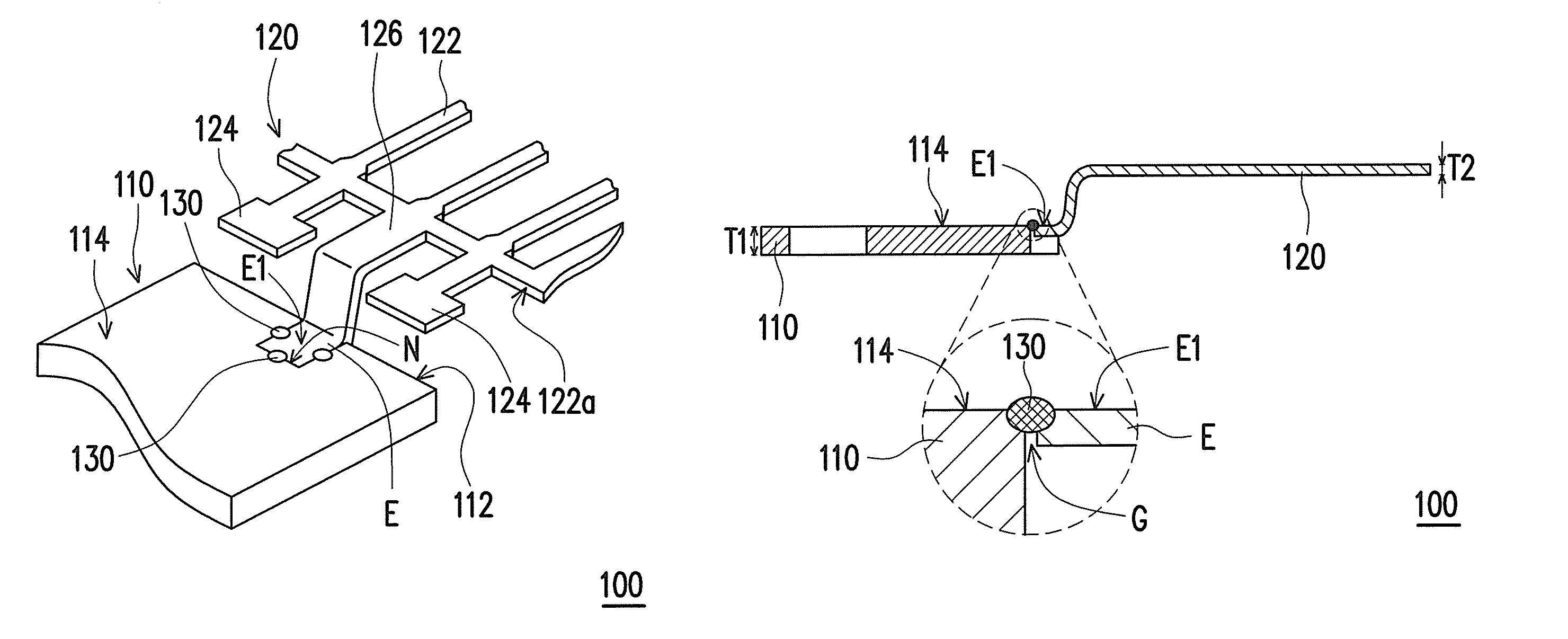
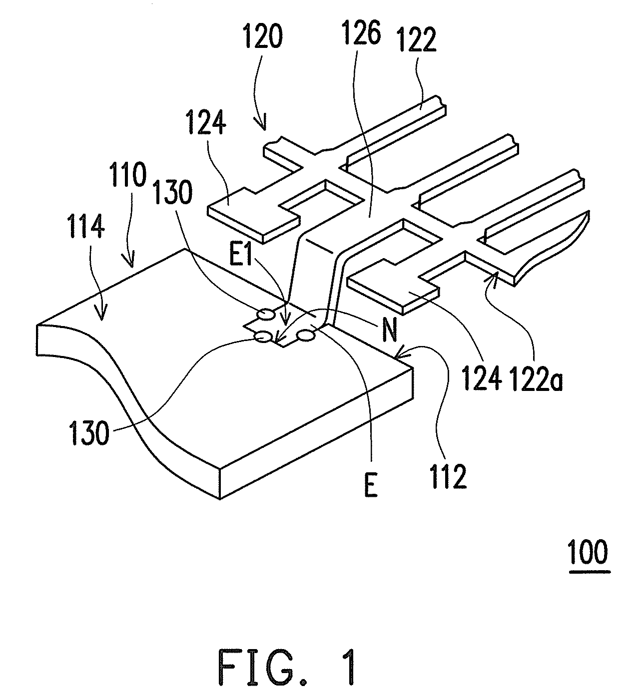
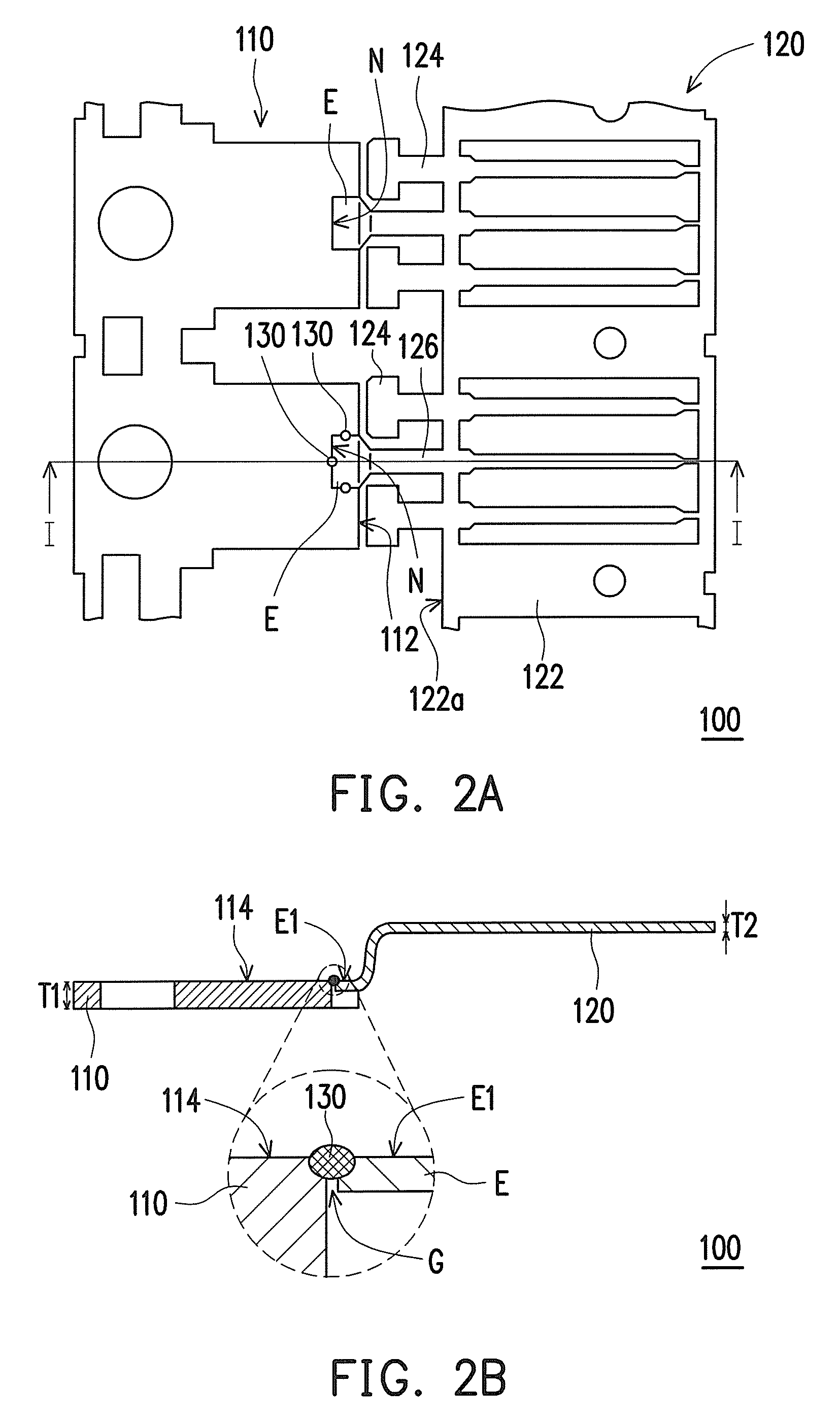
FIG. 1 is a schematic three-dimensional view of a leadframe according to an embodiment of the present invention. FIG. 2A is a top view of the leadframe depicted in FIG. 1. FIG. 2B is a schematic cross-sectional view taken along a line I-I in FIG. 2A. FIG. 3 is a schematic three-dimensional view of a chip supporting plate and a lead forming plate of the leadframe depicted in FIG. 1. Here, the chip supporting plate and the lead forming plate are not yet welded.

Referring to FIGS. 1, 2A, and 2B, a leadframe 100 of the present embodiment includes a chip supporting plate 110, a lead forming plate 120, and a plurality of solder points 130. A notch N is formed on an edge 112 of the chip supporting plate 110. The thickness T2 of the lead forming plate 120 is less than the thickness T1 of the chip supporting plate 110.

The lead forming plate 120 includes a main body 122, a plurality of inner leads 124, and a connecting rod 126. The inner leads 124 and the connecting rod 126 are extended from a...


PUM


Abstract

A leadframe including a chip supporting plate, a lead forming plate, and solder points is provided. A notch is formed on an edge of the chip supporting plate. The thickness of the lead forming plate is less than the thickness of the chip supporting plate. The lead forming plate has a main body, inner leads, and a connecting rod. The inner leads and the connecting rod are extended from an edge of the main body. The connecting rod has an end portion fitting the notch. The solder points are located at the boundary between the end portion and the notch for structurally connecting the connecting rod and the chip supporting plate.

Description

CROSS-REFERENCE TO RELATED APPLICATIONThis application claims the priority benefit of P.R.C. patent application serial no. 200810212841.3, filed on Sep. 10, 2008. The entirety of the above-mentioned patent application is hereby incorporated by reference herein and made a part of specification.BACKGROUND OF THE INVENTION1. Field of the InventionThe present invention relates to a leadframe, and more particularly to a leadframe with different thicknesses.2. Description of Related ArtA wire bonding technology is a common chip packaging technology applied to electrically connect a chip to a carrier. To satisfy requirements for low pin counts, a leadframe is frequently used as a chip carrier in the wire bonding technology. In most cases, the leadframe includes a die base for accommodating the chip and a plurality of leads disposed around the die base. Since the leadframe is often made of processing metal thin plates, the thickness of the die base and the thickness of the leads in the lead...

Claims


Application Information

Patent Timeline
Patent Type & Authority Patents(United States)
IPC IPC(8): H01L23/48H01L23/495H01L29/78H01L29/739
CPCH01L23/49562H01L2924/0002H01L2924/00
Inventor LIU, SHENG-TSUNG
Owner ADVANCED SEMICON ENG INC
Why Eureka
Try Eureka