Resistance variable element, nonvolatile switching element, and resistance variable memory apparatus

a technology of resistance variable and nonvolatile switching elements, which is applied in the direction of digital storage, semiconductor devices, instruments, etc., can solve the problem of limiting the miniaturization of an existing flash memory using a floating ga

Active Publication Date: 2011-05-24
PANASONIC SEMICON SOLUTIONS CO LTD
View PDF21 Cites 7 Cited by
  • Summary
  • Abstract
  • Description
  • Claims
  • Application Information

AI Technical Summary

Benefits of technology

[0035]Since the present invention is configured as described above, it is possible to provide a novel resistance variable element which can be manufactured at a low temperature, and has a property that all the voltage pulses for writing have the same polarity (unipolar drivable), and a resistance variable memory apparatus using the resistive variable element.

Problems solved by technology

In response to such demands, it is said that there is a limitation on miniaturization of an existing flash memory using a floating gate.

Method used


Image

  • Resistance variable element, nonvolatile switching element, and resistance variable memory apparatus
  • Resistance variable element, nonvolatile switching element, and resistance variable memory apparatus
  • Resistance variable element, nonvolatile switching element, and resistance variable memory apparatus

Examples


embodiment 1

Configuration

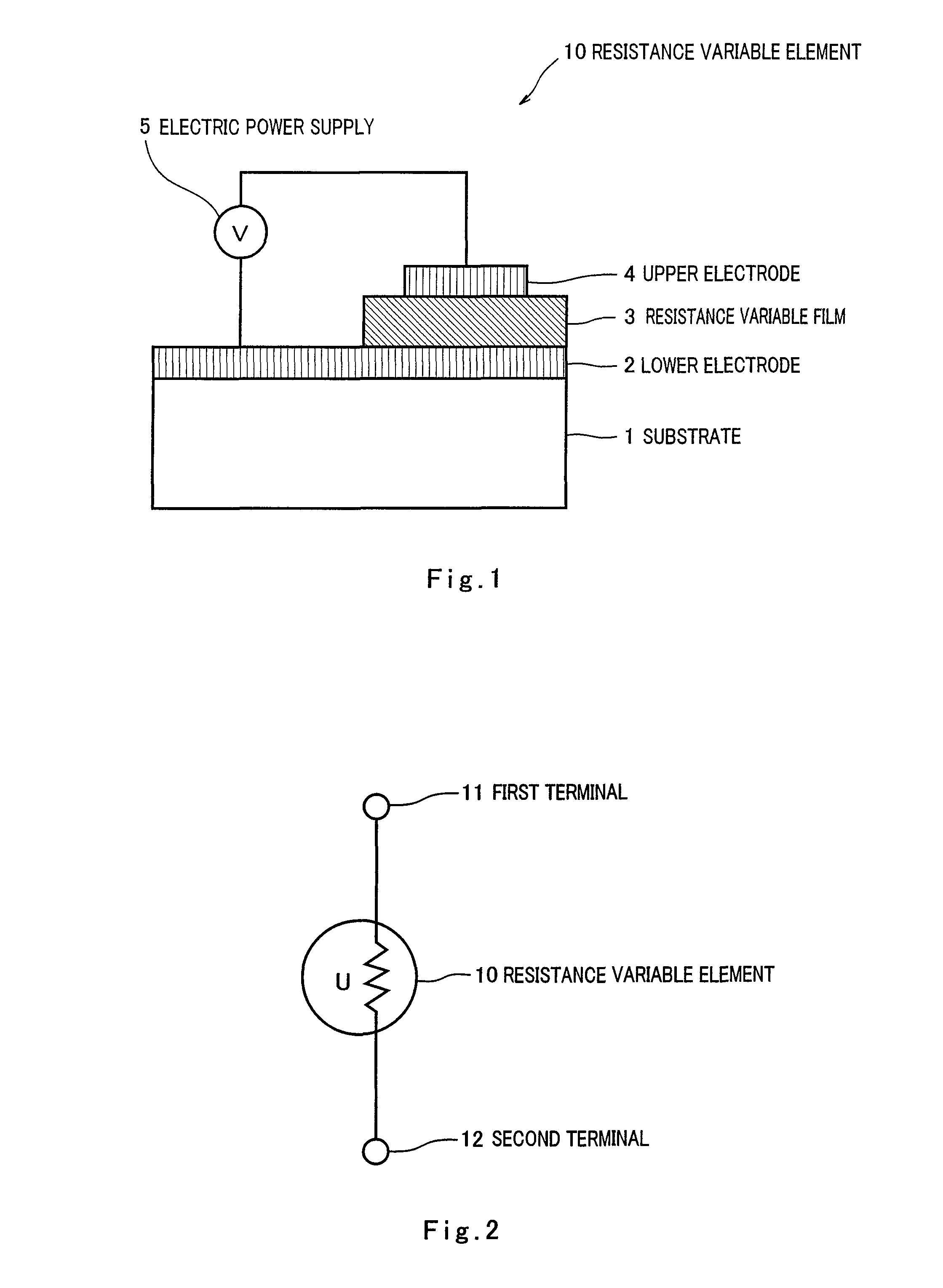
[0071]FIG. 1 is a schematic view illustrating an example of a configuration of a resistance variable element according to Embodiment 1 of the present invention. As shown in FIG. 1, a resistance variable element 10 of this embodiment comprises a substrate 1, a lower electrode 2 (first electrode) formed on the substrate 1, a resistance variable layer 3 formed on the lower electrode 2, and an upper electrode 4 (second electrode) formed on the resistance variable layer 3. The lower electrode 2 and the upper electrode 4 are respectively electrically connected to the resistance variable layer 3. The upper electrode 4 may be the first electrode, while the lower electrode 2 may be the second electrode.

[0072]The substrate 1 is formed of, for example, a silicon substrate.

[0073]The lower electrode 2 and the upper electrode 4 may be made of one or plural materials selected from a group consisting of, for example, Ag (silver), Au (gold), Pt (platinum), Ir (iridium), TiN (titanium ni...

example 1

[0109]A lower electrode (size: 20 μm×20 μm) comprising Pt was formed to have a thickness of 0.2 μm on a silicon substrate by sputtering. Next, a target of Ta was prepared, oxygen was mixed into argon with a predetermined flow rate ratio, and reactive sputtering was performed, thereby forming on the lower electrode 2 the resistance variable layer 3 which is expressed by a chemical formula of TaOX and has an amorphous structure. Then, using a mask and lithography, the resistance variable layer (size: 10 μm×10 μm, area: 100 μm2) which is expressed by a chemical formula of TaOX and has an amorphous structure was formed on the lower electrode. The resistance variable layer was formed under the room temperature without particularly heating the substrate. The size of the portion where the lower electrode contacts the resistance variable layer was 10 μm×10 μm (area: 100 μm2). The thickness of the resistance variable layer was 100 nm. Further, an upper electrode (size: 2 μm×2 μm) comprising ...

example 2

[0116]In Example 2, a resistance variable element was manufactured and writing and reading out were carried out in manners similar to those in Example 1 except that different parameters were used.

[0117]To be specific, in Example 2, the flow rate ratio of the oxygen gas during the reactive sputtering was controlled so that the value of X in TaOX which forms the resistance variable layer became 1.9. The value of X was verified by the RBS (Rutherford back scattering) method. As a result of the verification, the value of X was 1.9.

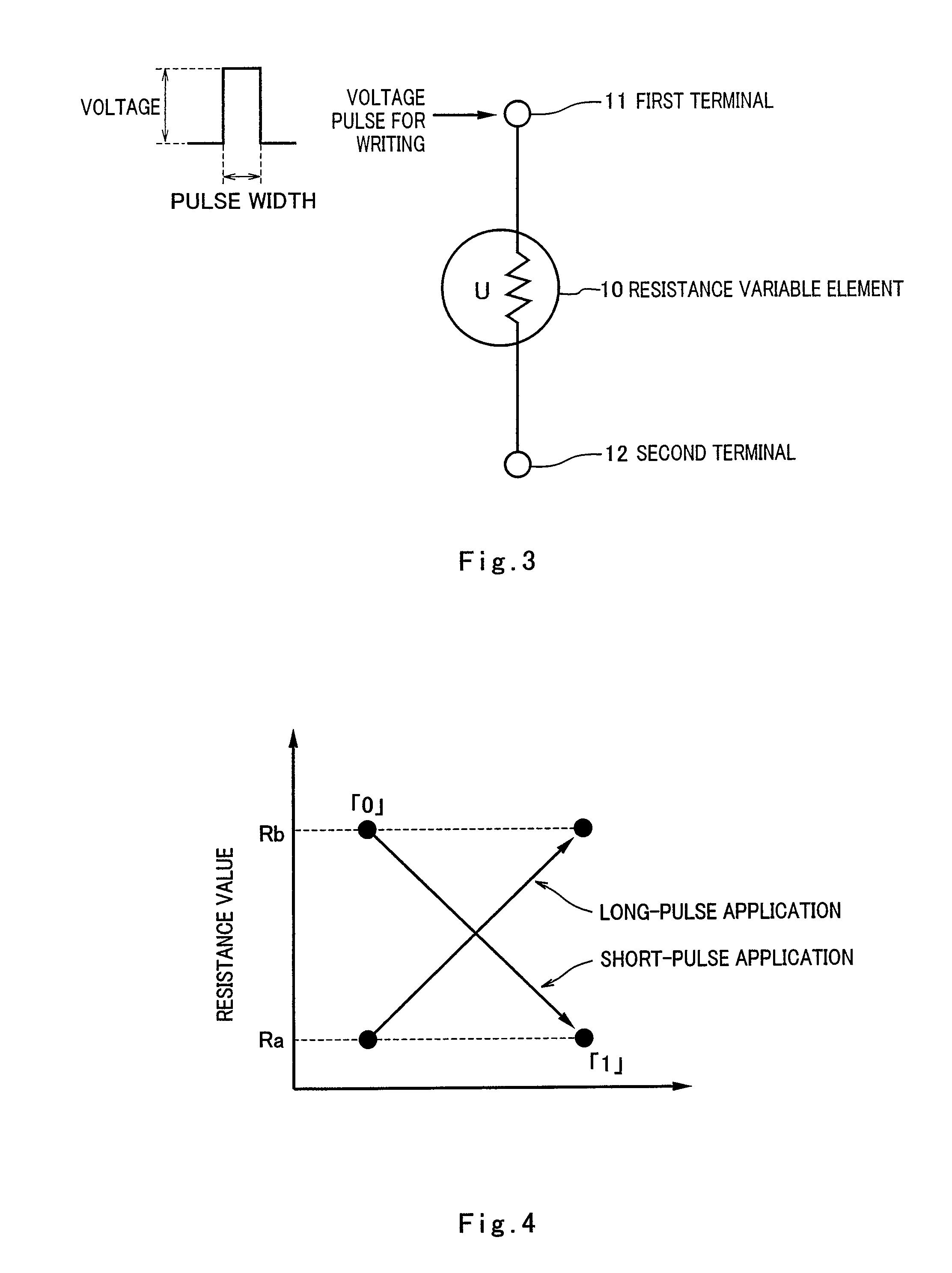
[0118]The resistance variable element obtained by the above described method was connected to an electric power supply, and a short pulse (voltage: +5.0V, pulse width: 100 ns) and a long pulse (voltage: +2.5V, pulse width: 100 μs) were alternately applied. A voltage with which the electric potential of the upper electrode became higher than that of the lower electrode was a plus voltage.

[0119]The resistance value of the resistance variable element was measured...


PUM


Abstract

A resistance variable element comprises a first electrode (2), a second electrode (4), and a resistance variable layer (3) which is disposed between the first electrode and the second electrode, and electrically connected to the first electrode and the second electrode, wherein the resistance variable layer comprises material including TaOX (1.6≦X≦2.2), an electric resistance between the first electrode and the second electrode is lowered by application of a first voltage pulse having a first voltage between the first electrode and the second electrode, and the electric resistance between the first electrode and the second electrode is increased by application of a second voltage pulse having a second voltage of the same polarity as the first voltage, between the first electrode and the second electrode.

Description

RELATED APPLICATIONS[0001]This application is the US National Phase under 35 U.S.C. §371 of International Application No. PCT / JP2008 / 00768 filed on Mar. 27, 2008, which claims the benefit of Japanese Application No. JP2007-101506 filed on Apr. 9, 2007, the disclosures of which Applications are incorporated by reference herein.TECHNICAL FIELD[0002]The present invention relates to a resistance variable element and a resistance variable memory apparatus. More particularly, the present invention relates to a resistance variable element, a nonvolatile switching element, and a resistance variable memory apparatus, whose electric resistances vary according to applied voltage pulses.BACKGROUND ART[0003]With the advancement of digital technologies in electronic devices, demands for an increase in a capacity of a nonvolatile resistance variable element, a reduction in writing electric power, a reduction in write / read-out time, and longer life have been increasing, for storing data such as ima...

Claims


Application Information

Patent Timeline
Patent Type & Authority Patents(United States)
IPC IPC(8): G11C11/00
CPCG11C13/0007G11C13/0069H01L45/04H01L27/101H01L45/1233H01L45/146H01L45/1625G11C2013/009G11C2013/0092G11C2213/32H01L27/2409G11C2213/72H10B63/20H10N70/20H10N70/026H10N70/8833H10N70/826
Inventor MURAOKA, SHUNSAKUOSANO, KOICHIFUJII, SATORU
Owner PANASONIC SEMICON SOLUTIONS CO LTD
Why Eureka
Try Eureka