Analysis techniques for multi-level memory

a multi-level memory and analysis technique technology, applied in the field of integrated circuit quality control systems and methods, can solve the problems of improving yield and low yield of final memory cell products, and achieve the effect of easy interpretation and understanding and convenient us

Active Publication Date: 2011-05-31
ONTO INNOVATION INC
View PDF12 Cites 4 Cited by
  • Summary
  • Abstract
  • Description
  • Claims
  • Application Information

AI Technical Summary

Benefits of technology

[0022]One embodiment of the system and method for analysis of multi-level memory cell devices and embedded multi-level memory in system-on-chip integrated circuits in accordance with the present invention provides many advantages over conventional analysis systems and techniques, which make the multi-level memory defect analysis system and method in accordance with the present invention more useful to semiconductor manufacturers. The multi-level memory defect analysis system and method in accordance with the various embodiments of the present invention identify random and systematic failure mechanisms. The system may be fully automated and is easy to use, so that no extra training is necessary to make use of the multi-level memory defect analysis system. The system generates an output preferably in the form of a failed bit analysis report that is easy to interpret and understand.
[0023]In accordance with one preferred embodiment of the present invention, a system and method for analyzing defects in multi-level memory cell devices and embedded multi-level memory in system-on-chip integrated circuits manufactured using a semiconductor fabrication process are provided. One embodiment of the multi-level memory defect analysis system and method in accordance with the present invention may receive a defect data set from a memory tester that extracts bits from memory chips. When a defect data set is received, an automated test engineering system running a memory test program analyzes the defect data set to generate one or more fail bit locations and one or more fail states of the memory. The multi-level memory defect analysis system and method in accordance with one embodiment of the present invention then classify failed bits or patterns comprising a vertical fail pattern, whereby after being classified, each memory cell failure vertical fail pattern has three data attributes comprising fail type, a number of fail bits / states, and a sequence of the fail states. The vertical fail pattern may comprise a single fail state or multi-state fail. The multi-state fail may be a continuous-states fail, discontinuous-states fail, or all-state fail. The multi-level memory defect analysis system and method in accordance with another embodiment of the present invention also preferably enable classification of failed bits or patterns comprising a lateral fail pattern. The lateral fail pattern may comprise a gradual fail pattern, periodic fail pattern, or random fail pattern. Preferably, the multi-level memory defect analysis system and method generate a defect analysis report of failed bits or patterns and / or display failed bits or patterns. The multi-level memory defect analysis system and method in accordance with various embodiments of the present invention may generate a three-dimensional classification, produce a correlation, provide zonal analysis of memory blocks, reconfigure memory device capacity, and implement redundancy. The correlation provides correlation of defects to fail bits / patterns, correlation of Wafer Electrical Test or Wafer Acceptance Test data to fail bits / patterns, correlation of sort parametric data to fail bits / patterns, or correlation of in-line measurement data to fail bits / patterns. The multi-level memory defect analysis system and method in accordance with the present invention provide a defect analysis tool for analysis of multi-level memory cell devices and embedded multi-level memory in system-on-chip integrated circuits that is more powerful and flexible than conventional tools.

Problems solved by technology

The occurrence of defects may cause lower yield in the final memory cell product, where yield may be defined as the number of functional memory cell devices produced by the process as compared to the theoretical number of devices that could be produced assuming no bad devices.
Improving yield is a critical issue in the semiconductor manufacturing industry.

Method used


Image

  • Analysis techniques for multi-level memory
  • Analysis techniques for multi-level memory
  • Analysis techniques for multi-level memory

Examples


Embodiment Construction

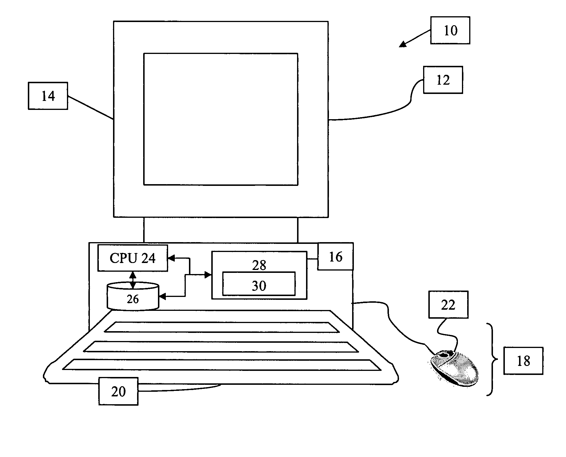
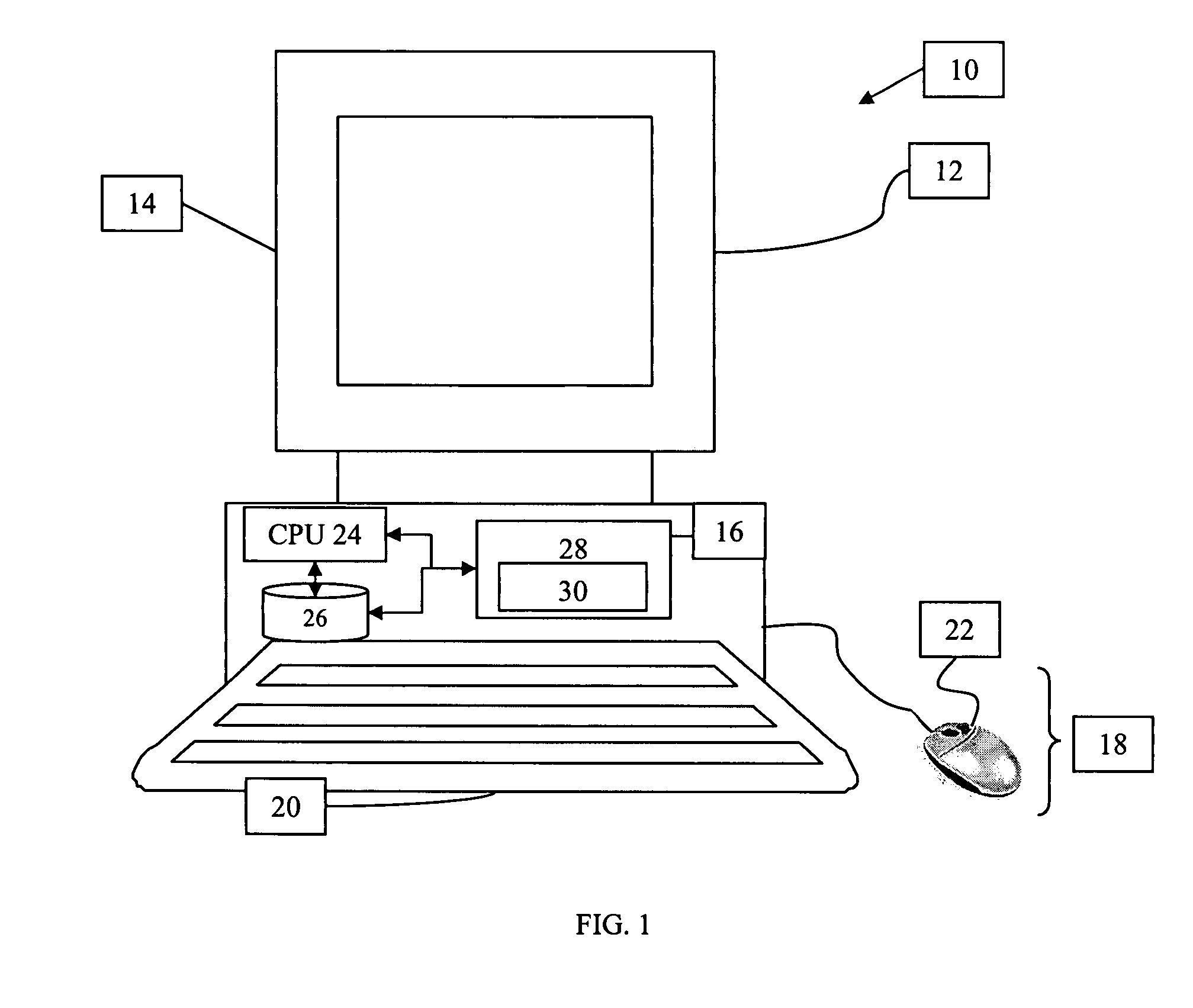
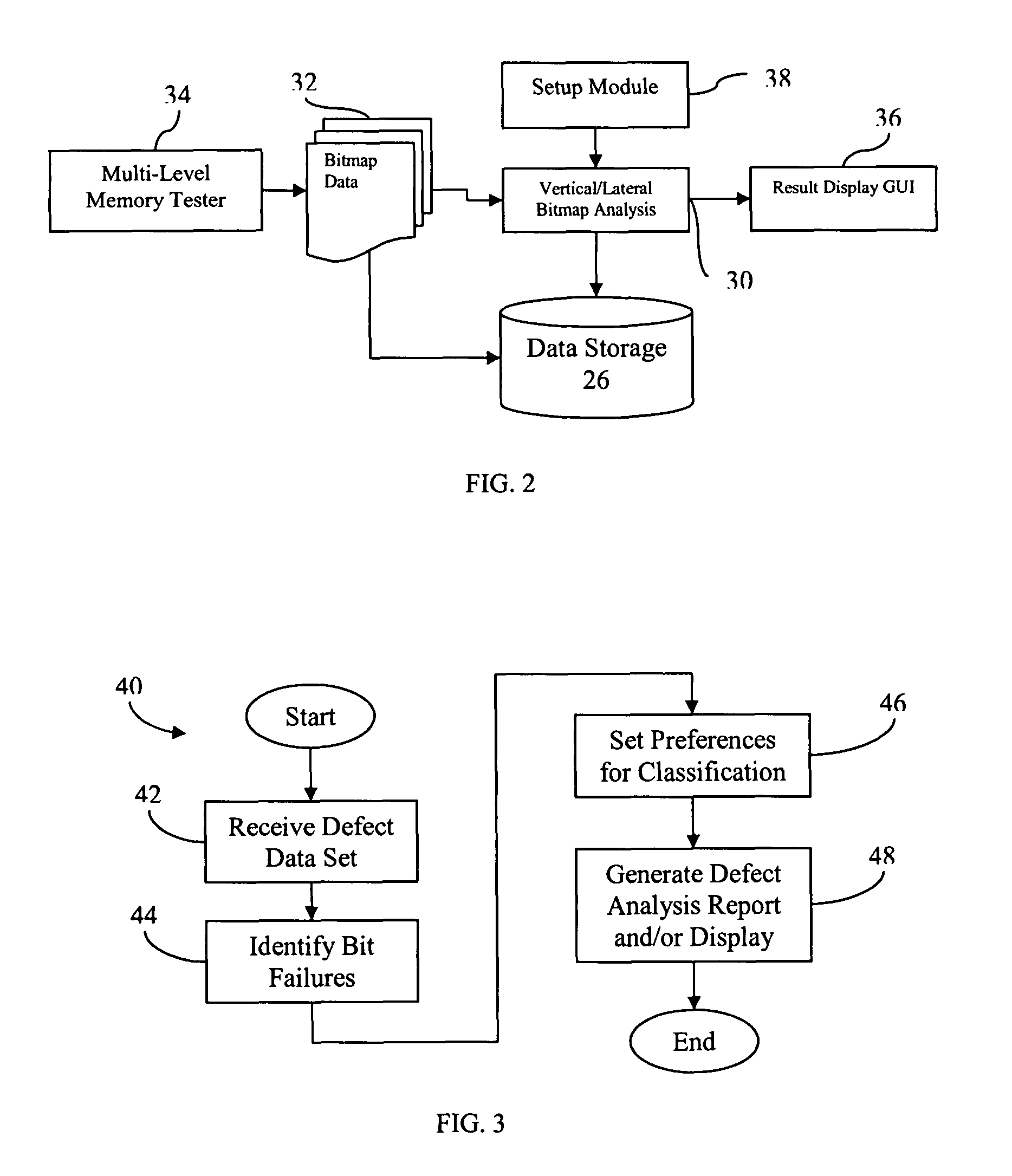
[0032]The present invention is particularly applicable to a computer-implemented software-based defect analysis system and method for multi-level memory cell devices and embedded multi-level memory in system-on-chip integrated circuits, and it is in this context that the various embodiments of the present invention will be described. It will be appreciated, however, that the multi-level memory defect analysis system and method in accordance with the present invention have greater utility, since they may be implemented in hardware or may incorporate other modules or functionality not described herein.

[0033]FIG. 1 is a block diagram illustrating an example of a multi-level memory defect analysis system 10 in accordance with one embodiment of the present invention implemented on a personal computer 12. In particular, the personal computer 12 may include a display unit 14, which may be a cathode ray tube (CRT), a liquid crystal display, or the like; a processing unit 16; and one or more...


PUM


Abstract

A system and method for defect analysis of multi-level memory cell devices and embedded multi-level memory in system-on-chip integrated circuits are disclosed wherein a defect data set is input into the system. When a defect data set is received, an automated test engineering system running a memory test program analyzes the defect data set to generate one or more fail bit locations and one or more fail states of the memory. The multi-level memory defect analysis system and method then classify failed bits or patterns comprising a vertical fail pattern, whereby after being classified, each memory cell failure vertical fail pattern has three data attributes comprising fail type, a number of fail bits / states, and a sequence of the fail states. The vertical fail pattern may comprise a single fail state or multi-state fail. The multi-state fail may be a continuous-states fail, discontinuous-states fail, or all-state fail. The multi-level memory defect analysis system and method may additionally enable classification of failed bits or patterns comprising a lateral fail pattern. The lateral fail pattern may be a gradual fail pattern, periodic fail pattern, or random fail pattern.

Description

BACKGROUND OF THE INVENTION[0001]1. Field of the Invention[0002]The present invention relates generally to systems and methods for quality control of integrated circuits manufactured by a semiconductor manufacturing process and, more particularly, to a system and method for analyzing defects in multi-level memory cell devices and embedded multi-level memory in system-on-chip integrated circuits manufactured using a semiconductor fabrication process.[0003]2. Description of the Prior Art[0004]A standard memory cell typically stores one bit of information by storing one of two levels of electrical charge in its storage cell, namely, full charge or no charge. Newer memory devices, sometimes referred to as multi-level cell devices, can store more than one bit per cell, by storing two or more levels of electrical charge per memory cell.[0005]Traditionally, with standard memory cell analysis, one would analyze the failed memory cells by assigning each cell to be a failed cell or a passed c...

Claims


Application Information

Patent Timeline
Patent Type & Authority Patents(United States)
IPC IPC(8): G11C29/00
CPCG11C29/10G11C29/56008G11C29/56
Inventor HO, TOM T.BUCKHEIT, JONATHAN B.WANG, WEIDONG
Owner ONTO INNOVATION INC
Why Eureka
Try Eureka