Nonvolatile semiconductor memory device

a semiconductor and memory device technology, applied in semiconductor devices, semiconductor/solid-state device details, capacitors, etc., can solve the problems of large defect size of high-k insulating film and interface, and it is not possible to improve both high low electric field leakage current characteristics at the same time. , to achieve the effect of lowering the dielectric constant and high barrier heigh

Active Publication Date: 2011-06-07
KIOXIA CORP
View PDF18 Cites 37 Cited by
  • Summary
  • Abstract
  • Description
  • Claims
  • Application Information

AI Technical Summary

Benefits of technology

[0014]A nonvolatile semiconductor memory device according to an aspect of the present invention comprises source / drain layers provided separately from each other on a surface of a semiconductor substrate, a first insulating film provided on a channel between the source / drain layers, a charge storage layer provided on the first insulating film, a second insulating film which is provided on the charge storage layer, and a control gate electrode provided on the second insulating film. A dielectric constant, a barrier height and an average coordination number of the second insulating film vary continuously in a thickness direction, and a middle part of the second insulating film in the thickness direction where the dielectric constant and the barrier height result in external values is formed of one of oxide and oxynitride whose compositional ratio of silicon is larger than other parts of the second insulating film.

Problems solved by technology

However, the High-k insulating film involves larger amount of defects within a film and an interface, as compared with the insulating film of a silicon oxide film system.
As described above, in the conventional second insulating film, there is a problem that it is not possible to improve both high electric field leakage current characteristics and low electric field leakage current characteristics simultaneously.

Method used


Image

  • Nonvolatile semiconductor memory device
  • Nonvolatile semiconductor memory device
  • Nonvolatile semiconductor memory device

Examples


embodiment 1

(1) Embodiment 1

[0133]FIG. 5 shows a memory cell of the embodiment 1.

[0134]FIG. 5 (a) is a cross sectional view along the channel length direction, and FIG. 5 (b) is a cross sectional view along the channel width direction. Additionally, FIG. 6 shows a structure of FIG. 5 (a) in detail.

[0135]On a surface of a p type silicon substrate (including wells) 101, two source / drain diffusion layers 110 are provided separately from each other. Space between the source / drain diffusion layers 110 is a channel region, and when the memory cell becomes ON state, a channel for making the two source / drain diffusion layers 110 electrically conductive is formed in the channel region.

[0136]On the channel region, as the first insulating film (tunnel insulating film), for instance, a silicon oxide film (SiO2) 102 with a thickness of 4 nm is provided. On the first insulating film 102, as the charge storage layer, for instance, a silicon nitride film (Si3N4) 103 with a thickness of 6 nm is provided.

[0137]O...

embodiment 2

(2) Embodiment 2

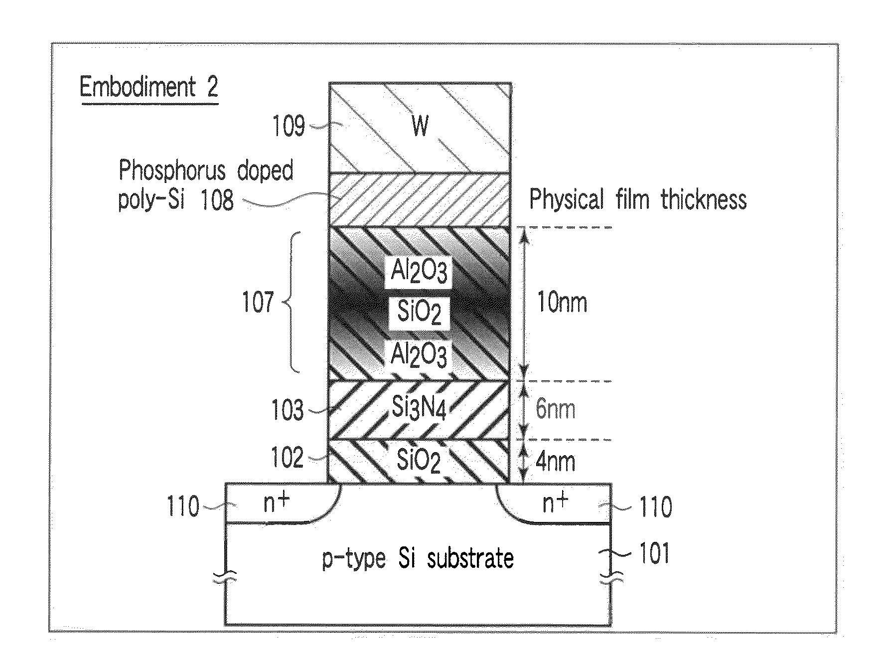
[0211]FIG. 19 shows a cross sectional view of a memory cell in the channel length direction of the embodiment 2. Note that in FIG. 19, the same symbols are assigned to the same parts as in FIG. 6, and their detailed description is omitted.

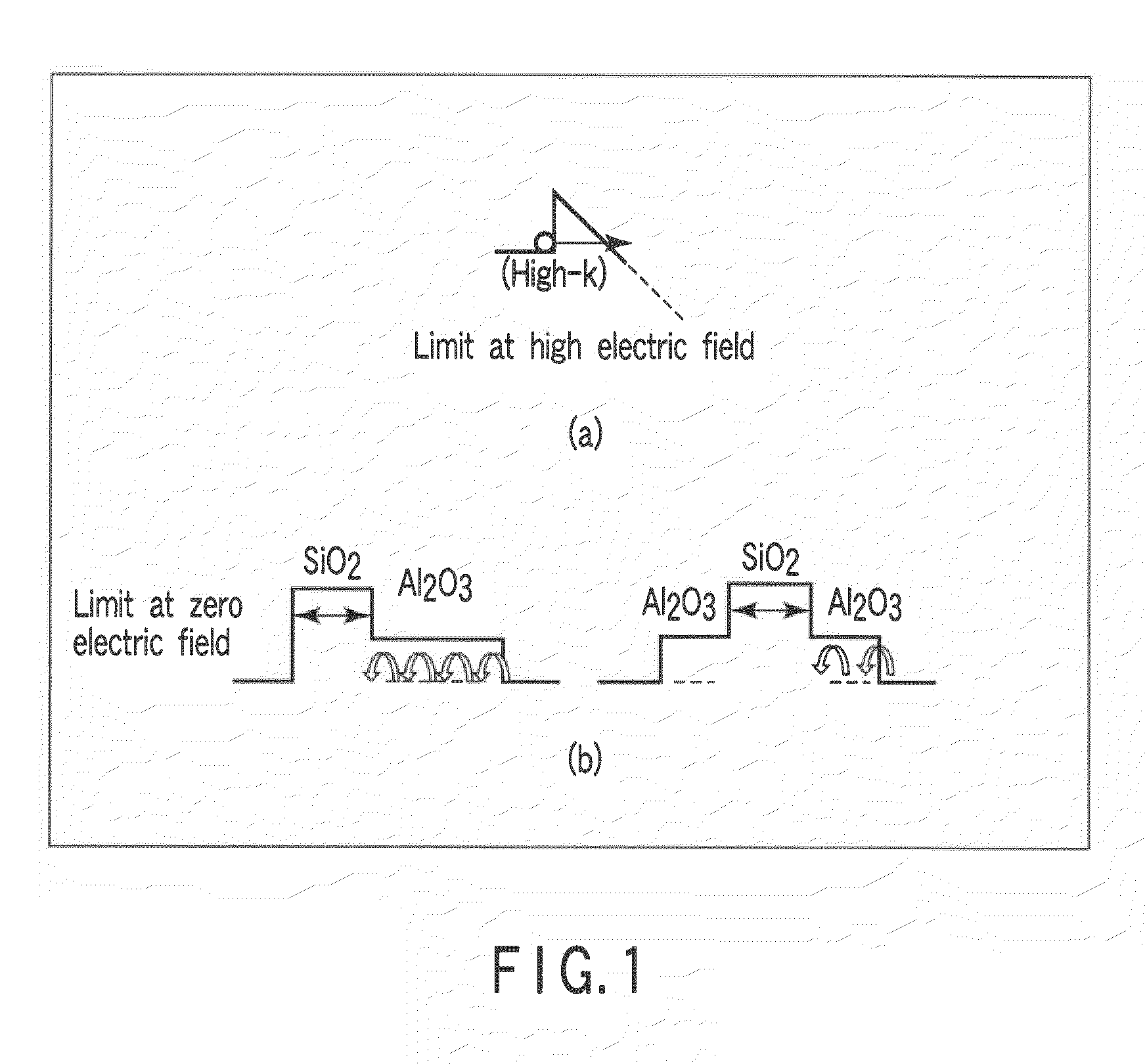
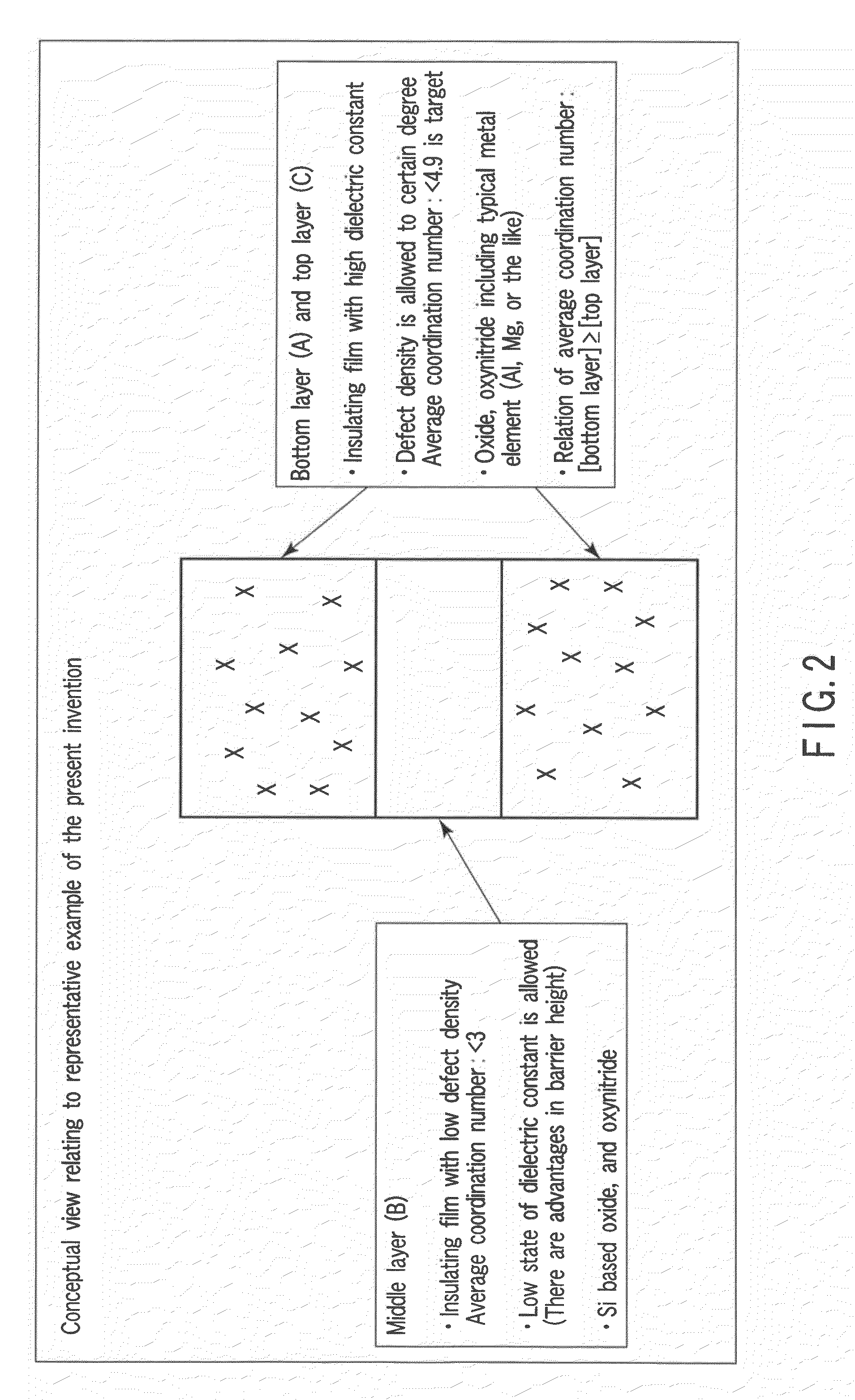
[0212]The present embodiment differs from the previously described embodiment 1 in that the second insulating film is composed of an insulating film having continuous compositional variation, instead of forming the clearly distinguishable three layers of the bottom layer (A), the middle layer (B), and the top layer (C).

[0213]On a surface of p-type silicon substrate (including wells) 101, two source / drain diffusion layers 110 are provided separately from each other. On the channel region between the source / drain diffusion layers 110, as the first insulating film (tunnel insulating film), for instance, the silicon oxide film (SiO2) 102 with a thickness of 4 nm is provided. On the first insulating film 102, as the charge storage layer,...

embodiment 3

(3) Embodiment 3

[0224]FIG. 20 shows a cross sectional view of the memory cell of an embodiment 3 in the channel length direction. Note that in FIG. 20, the same symbols are assigned to the same parts as in FIG. 6, and their detailed description will be omitted.

[0225]The present embodiment differs from the previously described embodiment 1 in that a silicon oxynitride film (SiON: (SiO2)x(Si3N4)1-x for the compositional expression) is used instead of the silicon oxide film (SiO2) as the middle layer of the second insulating film.

[0226]On a surface of p-type silicon substrate (including wells) 101, two source / drain diffusion layers 110 are provided separately from each other. On the channel region between the source / drain diffusion layers 110, as the first insulating film (tunnel insulating film), for instance, the silicon oxide film (SiO2) 102 with a thickness of 4 nm is provided. On the first insulating film 102, as the charge storage layer, for instance, the silicon nitride film (Si...


PUM


Abstract

A nonvolatile semiconductor memory device includes a charge storage layer on a first insulating film, a second insulating film which is provided on the charge storage layer, formed of layers, and a control gate electrode on the second insulating film. The second insulating film includes a bottom layer (A) provided just above the charge storage layer, a top layer (C) provided just below the control gate electrode, and a middle layer (B) provided between the bottom layer (A) and the top layer (C). The middle layer (B) has higher barrier height and lower dielectric constant than both the bottom layer (A) and the top layer (C). The average coordination number of the middle layer (B) is smaller than both the average coordination number of the top layer (C) and the average coordination number of the bottom layer (A).

Description

CROSS-REFERENCE TO RELATED APPLICATIONS[0001]This application is based upon and claims the benefit of priority from prior Japanese Patent Application No. 2007-250291, filed Sep. 26, 2007, the entire contents of which are incorporated herein by reference.BACKGROUND OF THE INVENTION[0002]1. Field of the Invention[0003]The present invention relates to a nonvolatile semiconductor memory device having a memory cell with stack gate structure, and particularly, is used for a fine NAND type flash memory.[0004]2. Description of the Related Art[0005]A stack gate structure of a memory cell in the NAND type flash memory is formed of a first insulating film formed on a Si substrate, a charge storage layer formed on the first insulating film, and further a second insulating film formed on the charge storage layer. The first insulating film is named as “a tunnel insulating film”, and when applying high electric field to this insulating film, exchanging charges between the Si substrate and the char...

Claims


Application Information

Patent Timeline
Patent Type & Authority Patents(United States)
IPC IPC(8): H01L29/792
CPCH01L21/28282H01L27/115H01L27/11568H01L29/42324H01L29/4234H01L29/513H01L29/517H01L29/792H01L29/788H01L27/10805H01L28/40H01L29/4966H01L29/7881H01L29/40117H10B43/30H10B69/00H01L28/60H10B12/30H10B43/35H01L21/283H01L21/76224H01L23/528H01L29/0649H01L29/4925H01L29/518
Inventor YASUDA, NAOKI
Owner KIOXIA CORP
Why Eureka
Try Eureka