Multiple indium implant methods and devices and integrated circuits therefrom

a technology of indium implants and integrated circuits, which is applied in the direction of semiconductor devices, electrical apparatus, transistors, etc., to achieve the effects of reducing short-channel effects, reducing impurity scattering, and increasing v

Active Publication Date: 2011-06-14
TEXAS INSTR INC
View PDF7 Cites 117 Cited by
  • Summary
  • Abstract
  • Description
  • Claims
  • Application Information

AI Technical Summary

Problems solved by technology

The Present Inventors have realized a problem with using In for NMOS devices is that In achieves a state of solid solubility at a point below the concentration required to generally reach worst case leakage currents.

Method used


Image

  • Multiple indium implant methods and devices and integrated circuits therefrom
  • Multiple indium implant methods and devices and integrated circuits therefrom
  • Multiple indium implant methods and devices and integrated circuits therefrom

Examples


examples

[0030]The following non-limiting Examples serve to illustrate selected embodiments of the invention. It will be appreciated that variations in proportions and alternatives in elements of the components shown will be apparent to those skilled in the art and are within the scope of embodiments of the present invention.

[0031]FIG. 3A shows as implanted In profiles into silicon for an exemplary first (shallower) In implant (dose 2.0×1013 cm−2 at 70 keV) and second In implant (dose 2.0×1013 cm−2 at 90 keV) according to an embodiment of the invention. Using the advanced anneals described above such as RTA, flash or laser anneals, which all generally provide a high temperature (e.g. 950 to 1050° C.) for a very short time (e.g. <10 seconds at the high temperature) the final In profiles in the completed NMOS devices are expected to remain significantly similar to the as-implanted In profiles shown in FIG. 3A.

[0032]The as implanted profile for a conventional B implant (dose 1.6×1013 cm−2 at 15...


PUM


Abstract

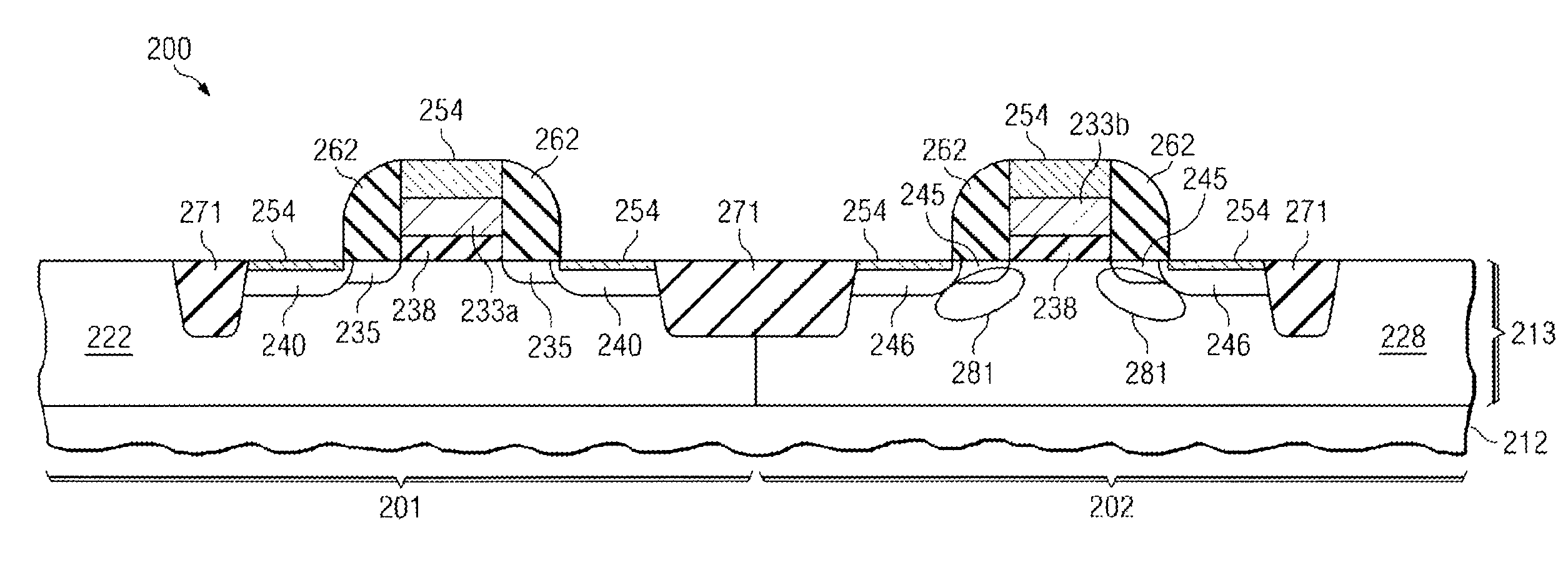
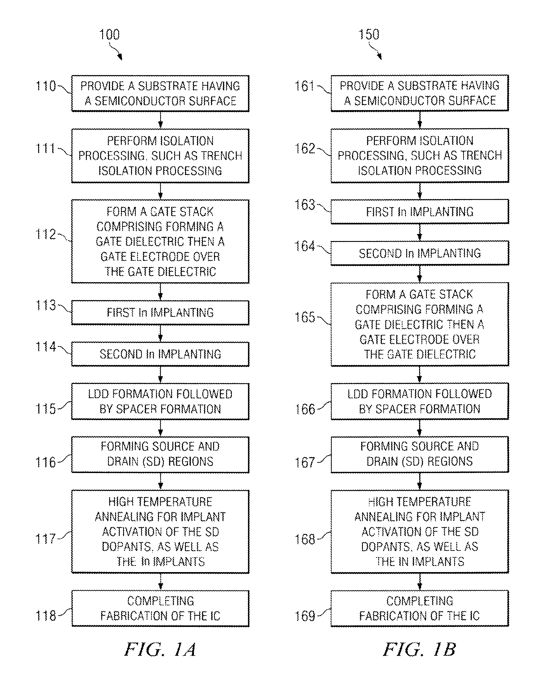
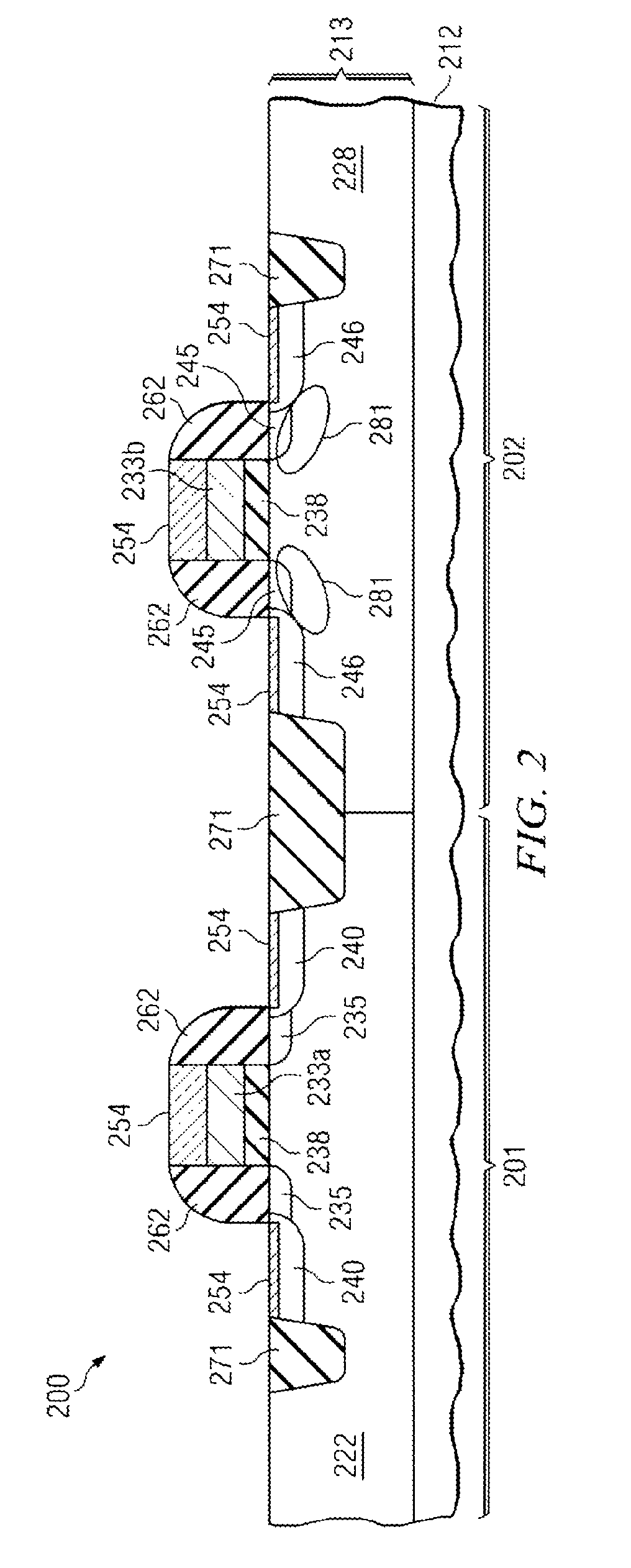
An integrated circuit (IC) includes at least one NMOS transistor, wherein the NMOS transistor includes a substrate having a semiconductor surface, and a gate stack formed in or on the surface including a gate electrode on a gate dielectric, wherein a channel region is located in the semiconductor surface below the gate dielectric. A source and a drain region are on opposing sides of the gate stack. An In region having a retrograde profile is under at least a portion of the channel region. The retrograde profile includes (i) a surface In concentration at a semiconductor surface interface with the gate dielectric of less than 5×1016 cm−3, (ii) a peak In concentration at least 20 nm from the semiconductor surface below the gate dielectric, and wherein (iii) the peak In concentration is at least two (2) orders of magnitude higher than the In concentration at the semiconductor surface interface. A method to form an IC including at least one NMOS transistor includes implanting a first In implant at a first energy and a second In implant at a second energy, wherein the first In implant together with the second In implant form an In region having a retrograde profile under at least a portion of the channel region, and wherein the second energy is at least 5 keV more than the first energy.

Description

FIELD OF THE INVENTION[0001]Embodiments of the present invention relate to methods for manufacturing MOS devices and integrated circuits (ICs) therefrom, more particularly to NMOS devices that include Indium implants under at least a portion of the channel region of the device.BACKGROUND[0002]The field effect transistor (FET) is a common element of an IC. In general, when fabricating multiple FETs of similar size, it is desired that a performance characteristic such as threshold voltage (Vt) be matched between devices. In general, the Vt tends to decrease in response to reduced gate length. As gate electrode lengths approach dimensions less than 100 nanometers (nm), what is seen is that the Vt drops off or decreases rapidly. Therefore, even a small change in the gate electrode length (e.g., a 10 nanometer difference from a targeted length), can significantly affect the Vt.[0003]Ideally, the Vt should be constant over a range of gate lengths about a target gate length to account for ...

Claims


Application Information

Patent Timeline
Patent Type & Authority Patents(United States)
IPC IPC(8): H01L21/336
CPCH01L21/26513H01L21/823412H01L21/823807H01L29/7833H01L29/66537H01L29/6659H01L29/1083H01L29/66507
Inventor KOHLI, PUNEETMEHROTRA, MANOJ
Owner TEXAS INSTR INC
Why Eureka
Try Eureka